

- News
15 March 2013
Textured ZnO improves performance of III-V on germanium solar cells
National Formosa University in Taiwan has developed a liquid-phase deposition (LPD) process of textured zinc oxide on III-V semiconductor to provide improved absorption of multi-junction solar cells [Po-Hsun Lei et al, J. Phys. D: Appl. Phys., vol46, p125105, 2013].
The textured layer reduces reflection of the incident light over a broad band of wavelengths (300-1000nm). Traditional anti-reflective coatings tend to be wavelength selective. The researchers were seeking a low-cost process to produce randomly textured surfaces as a means to improve solar cell light absorption performance.
The gallium indium phosphide/indium gallium arsenide/germanium (GaInP/InGaAs/Ge) solar cell material formation process consisted of metal-organic chemical vapor deposition (MOCVD) on germanium for the active material and a liquid-phase deposition in a Teflon vessel in a controlled-temperature water bath for the textured zinc oxide layer (Figures 1 and 2).
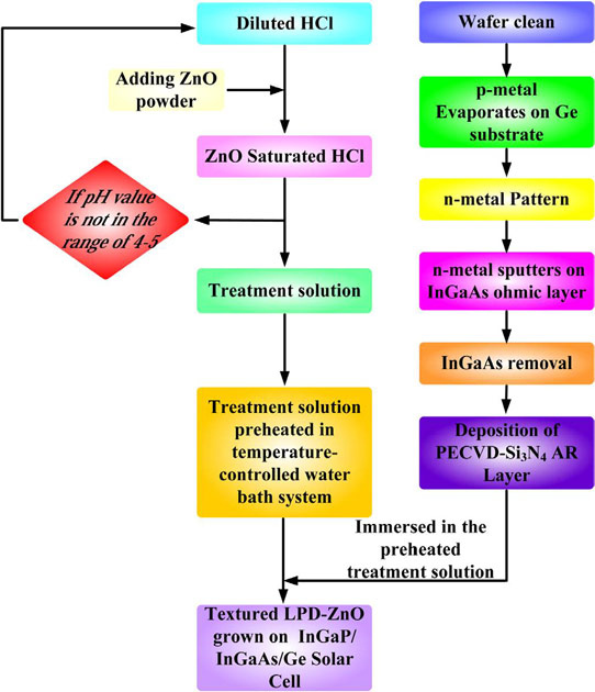
Figure 1: Flow chart for the LPD-ZnO process (left side) and fabrication of GaInP/(In)GaAs/Ge solar cells (right side).
The epitaxial material was cut up into 5mm x 5mm square chips. The ohmic p-contact was made to the back of the Ge substrate with a gold/zinc/silver/gold alloy. The ohmic n-electode structure consisted of germanium-gold/nickel/gold on the n-InGaAs top layer. A ridge n-contact was made by partially exposing regions of n-type aluminium indium phosphide (n-AlInP) window layer underneath by etching into the n-InGaAs.
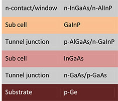 Figure 2: MOCVD heterostructure.
A silicon nitride (Si3N4) anti-reflective coating was applied to the n-AlInP using plasma-enhanced chemical vapor deposition (PECVD). The n-InGaAs is used for the electrical contact, but absorbs wavelengths that should be converted by the GaInP layer.
The ZnO was deposited on the silicon nitride. The researchers carried out a number of experiments to optimize the process parameters (pH, temperature) for control of layer thickness and root-mean-square (RMS) roughness. The textured ZnO layer consisted of nests of hexagonal flakes (Figure 3).
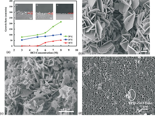
Figure 3: (a) Deposition rate of LPD-ZnO grown on Si3N4 as function of HCl concentration at various deposition temperatures, and FESEM images for LPD-ZnO grown at (b) 20°C, (c) 25°C and (d) 30°C. Insets of (a) show the cross-section FESEM images for LPD-ZnO grown at (a) 20°C, (b) 25°C and (c) 30°C at 6M HCl.
The aim of the ZnO layer was to reduce the reflection of light away from the solar cell. The optimum growth conditions for this were found to be 25°C with 6 mole/liter (M) hydrochloric acid solution. Also, the researchers performed simulations suggesting that the maximum enhancement for solar cells designed for a broad wavelength range would come from 95nm RMS roughness.
A bare solar cell without ZnO had a short-circuit current density of 12.5mA/cm2 and energy conversion of 24%. This is similar to the performance achieved by others, according to the researchers. With ZnO deposited from 6M solution at 25°C, these were increased to 14.22mA/cm2 and 29.8%, respectively.
Over a series of runs (Table 1), ZnO deposited from 6M solution at 25°C showed small variations in the character of the ZnO layer and in the performance of the solar cells. The RMS roughness of the ZnO layer varied in the range 90-100nm, while the pH value of the growth solution was kept in the range 4‑5.
Table 1: Performance of GaInP/(In)GaAs/Ge solar cells with textured LPD-ZnO window layer grown at 25°C in 6M HCl solution.
| Run no. | Short circuit current density (mA/cm2) | Open circuit voltage (V) | Conversion efficiency (%) | Fill factor |
| 1 | 14.25 | 2.43 | 29.71 | 0.85 |
| 2 | 14.35 | 2.43 | 29.65 | 0.84 |
| 3 | 15.09 | 2.41 | 29.64 | 0.81 |
| 4 | 14.92 | 2.34 | 28.43 | 0.81 |
| 5 | 14.57 | 2.42 | 29.78 | 0.84 |
| 6 | 15.00 | 2.42 | 29.79 | 0.82 |
| 7 | 14.85 | 2.41 | 29.81 | 0.83 |
| 8 | 14.81 | 2.41 | 28.92 | 0.811 |
| 9 | 14.73 | 2.39 | 29.50 | 0.83 |
| 10 | 14.73 | 2.39 | 29.63 | 0.84 |
| 11 | 14.81 | 2.39 | 29.81 | 0.84 |
| 12 | 14.72 | 2.38 | 29.80 | 0.85 |
The researchers comment: “The uniformity of the RMS roughness is extremely significant because this is the primary factor determining the absorbed light intensity or scattering between air and the textured LPD-ZnO.”
The variation in performance values were 3.31% for short-circuit current, 0.87% for open-circuit voltage, 3.75% for conversion efficiency, and 2.51% for fill factor.
The solar cells were also tested at operating temperatures up to 100°C. The variation in open-circuit voltage was 5.8mV/°C for cells without textured ZnO and 5.9mV/°C with. The respective rates for short-circuit current density were 7.9μA/°C-cm2 and 8.0μA/°C-cm2. The performance of solar cells tends to show that degraded energy conversion at high temperature and an increase in thermal resistance from added layers can be a concern for thermal management. The negligible changes in performance at raised temperature suggest that the ZnO layer does not significantly trap heat.
The researchers comment: “The introduction of the textured LPD-ZnO window layer for GaInP/(In)GaAs/Ge solar cells shows similar temperature characteristics as compared with those without the textured LPD-ZnO window layer. This may be attributed to the porosity of LPD-ZnO, which offers a path for reducing the thermal energy.”
ZnO LPD III-V on germanium solar cells Multi-junction solar cells
http://iopscience.iop.org/0022-3727/46/12/125105
The author Mike Cooke is a freelance technology journalist who has worked in the semiconductor and advanced technology sectors since 1997.
