

- News
22 March 2013
LayTec’s EpiNet 2 software tailored for growth analysis on patterned sapphire substrates
LayTec AG of Berlin, Germany (which makes in-situ metrology systems for thin-film processes, focusing on compound semiconductor and photovoltaic applications) says that, in the next few years, the use of patterned sapphire substrates (PSS) will increase due to the high light extraction efficiency. Following this trend, the firm says that its EpiNet 2 in-situ metrology software can be individually customized for various kinds of PSS, with users able to expand the substrate database by themselves.
LayTec’s Calibration Manual explains how to measure PSS reflectance in different pockets in one single calibration run. If required, LayTec also offers related customer training.
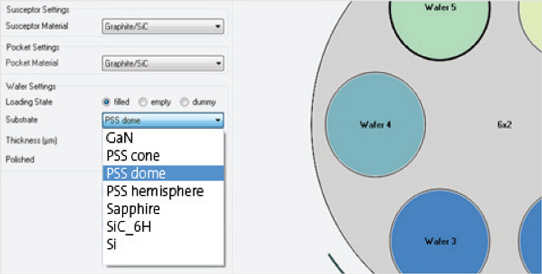
Figure 1: Extract of Run-Type’s Material Spec window of LayTec’s EpiNet 2 software, with customized database extended to additional PSS types.
Once the initial reflectance values of the PSS substrates are uploaded, the operator can choose the required substrate in the RunType’s Material Spec window (see Figure 1). As a result, all PSS wafers can be monitored with the same accuracy as standard sapphire substrates.
Figure 2 shows GaN growth on PSS. The initial 405nm reflectance on the bare PSS substrate is noisy because it senses the local non-uniformity of the PSS structure. As soon as the GaN buffer layer is thick enough, this noise reduces because the 405nm light no longer reaches the PSS pattern through the UV-absorbing GaN.
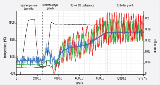
Figure 2: GaN growth on PSS measured by EpiCurveTT at FBH, Berlin, Germany: reflectance at 405nm (blue), 633nm (green), 950nm (red); True Temperature (black).
The increasing reflectance of all three wavelengths after about 4000s shows the coalescence process of GaN. After about 8050s, the 405nm reflectance remains stable at 15.5%, which is an indication of improvement in the GaN surface quality. However, the interference patterns of the 633/950nm reflectance look noisy during two-dimensional buffer growth. Clearly, the initial non-uniformity of the PSS structure causes a certain non-uniformity in GaN thickness.
Along with the customized database, EpiNet 2 also provides fitting of thin layers, wafer bow calculation, and many other features that are indispensable for growth on PSS, says LayTec.
