

- News
4 March 2013
BluGlass’ low-temperature RPCVD-grown p-type GaN films match MOCVD-grown electrical properties
Following its proof-of-concept achievement in late 2012, BluGlass Ltd of Silverwater, Australia says that it has produced p-type gallium nitride (GaN) films with industry-equivalent electrical properties using its proprietary low-temperature remote-plasma chemical vapor deposition (RPCVD) technology when grown on top of metal-organic chemical vapor deposition (MOCVD) GaN templates.
Spun off from the III-nitride department of Macquarie University of Sydney, Australia in 2005, BluGlass developed a low-temperature process using RPCVD to grow materials including gallium nitride (GaN) and indium gallium nitride (InGaN) on glass substrates, potentially offering cost, throughput and efficiency advantages for the production of LEDs.
BluGlass has now demonstrated p-GaN films grown at low temperature with electrical properties equivalent to films grown using the industry-standard MOCVD process. Specifically, compared with resistivity of less than 3Ohm-cm for a carrier concentration of 1017cm-3 for a typical MOCVD-grown p-GaN film, BluGlass’ RPCVD p-GaN film (grown on a commercial GaN template) yielded resistivity of 1Ohm-cm for a carrier concentration of 2x1017cm-3, according to room-temperature Hall measurement results.
BluGlass contracted The Australian National University (ANU) to independently measure and verify the electrical properties of the samples. The metal contacts required to perform the electrical measurements were prepared by the Australian National Fabrication Facility (ANFF).
Having demonstrated these material specifications BluGlass reckons it can now commence experiments targeting improved LED device efficiency using RPCVD-grown p-GaN layers, in order to demonstrate the commercial value of a low-temperature technology.
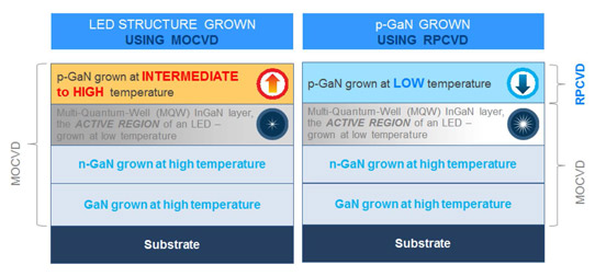
Figure 1: BluGlass targets low-temperature p-GaN as the first commercial opportunity for its RPCVD technology.
With a lower growth temperature than MOCVD, BluGlass reckons that its proprietary RPCVD technology has the potential to allow LED makers to create higher-performing devices by reducing the multi-quantum well or active region’s exposure to high temperatures, which currently leads to performance loss (see Figure 1).
“The technology team is making increasingly rapid progress in the development of our platform technology and technical milestones to prove the competitive advantages of the low-temperature RPCVD technology,” says CEO Giles Bourne.
“The next steps will see the technology focus on demonstrating that a low-temperature p-GaN layer can improve an LED’s efficiency over existing commercial devices,” says chief technology officer Dr Ian Mann. “We aim to do this by making a test LED device using RPCVD to grow p-GaN on top of an MOCVD-grown partial LED structure and to subsequently measure the light output of the device”.
BluGlass reports preliminary results on RPCVD-grown p-GaN
BluGlass' RPCVD grown GaN layers demonstrate reduced levels of key impurities
BluGlass grows high-quality crystalline GaN using low-temperature RPCVD
