
- News
11 June 2013
First wafer-scale heteroepitaxial growth of III-V nanowires on silicon
A team of researchers led by Kyoung Jin Choi, associate professor at South Korea’s Ulsan National Institute of Science and Technology (UNIST), and Xiuling Li, professor at University of Illinois in the USA, have developed what is claimed to be the first wafer-scale heteroepitaxial growth of III-V semiconducting nanowires on a silicon wafer (‘Wafer-Scale Production of Uniform InAsyP1-y Nanowire Array on Silicon for Heterogeneous Integration’, published online on 7 May in ACS Nano; DOI: 10.1021/nn4014774).
Supported by the Future-based Technology Development Program (Nano Fields) through the National Research Foundation of Korea (NRF) funded by the Ministry of Education, Science and Technology, the team demonstrated a method to epitaxially synthesize structurally and compositionally homogeneous and spatially uniform ternary InAsyP1-y nanowire on silicon on the wafer-scale using metal-organic chemical vapor deposition (MOCVD). The high quality of the nanowires is reflected in the narrow photoluminescence (PL) and x-ray peak width and low ideality factor in the InAsyP1-y nanowire/Si diode.
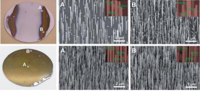 Picture: Optical and SEM images of the InAsyP1-y nanowire array.
High-aspect-ratio semiconductors have led to significant breakthroughs in conventional electrical, optical and energy-harvesting devices, say the researchers. Among such structures, III-V nanowires offer unique properties arising from their high electron mobility and absorption coefficients, as well as their direct bandgaps.
The common technique for creating a nanowire – i.e. vapor-liquid-solid (VLS) synthesis – can produce crystalline nanowires of some semiconductor materials, but metal catalysts (usually expensive noble metals) need to be used to initiate the VLS mechanism. Also, these metal catalysts are known to significantly degrade the quality of semiconductor nanowires by creating deep levels, limiting practical applications of nanowires in optoelectronic devices.
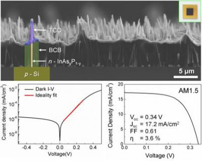 Picture: Electrical characterization of heterojunction solar cells composed of n- InAs0.7P0.3 nanowire array on p-Si (111) substrate.
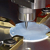
However, Choi’s group has developed a technique of growing III-V semiconductor nanowires without metal catalysts or nano-patterning. An Aixtron AIX 200 MOCVD system was used for growing the InAsyP1-y. A 2-inch Si (111) wafer was cleaned with buffer oxide etch for 1 minute and deionized (DI) water for 2 seconds. Then, the wafer was immediately dipped in poly-L-lysine solution (from Sigma-Aldrich Inc) for 3 minutes then rinsed in DI water for 10 seconds. The silicon substrate was then immediately loaded into the MOCVD system. The reactor pressure was lowered to 50mbar with 15liter/min of hydrogen gas flow. The reactor was then heated to growth temperature (570–630℃), and stabilized for 10 minutes.
“If we develop new technology which manages the density of nanowire and bandgap energy with further study, it is also possible to produce high-efficiency and low-cost large-scale solar cells,” concludes Choi.