


- News
7 June 2013
Improving dynamic performance of nitride HEMTs
Chinese Academy of Sciences’ Suzhou Institute of Nano-Tech and Nano-Bionics (SINANO) has extended its work on double-gated nitride semiconductor high-electron-mobility transistors (DG-HEMTs) [Guohao Yu et al, IEEE Electron Device Letters, vol. 34, p747, 2013]. In particular, the researchers applied large positive potentials to the top-gate of their structure, rather than merely trying to imitate the effects of source or gate field-plates.
The aim of the work was to find ways to avoid ‘current collapse’, where the device has reduced performance when switched compared with static characteristics. This has been a particular problem for nitride-based devices and needs to be tackled before such transistors can be used in power switching applications.
Various techniques for reducing current collapse have been suggested, such as surface passivation or field-plates connected to the source or gate to manipulate the electric field configuration. The effect of these is thought to be an alteration in the way charges are trapped on the surface or in the barrier layer of the nitride semiconductor heterostructure.
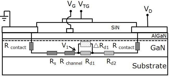
Figure 1: Schematic diagram showing the components of the dynamic on-resistance (RON_D) in a DG-HEMT with gallium nitride (GaN) buffer and aluminium gallium nitride (AlGaN) barrier. The gate-source distance was 5μm; gate-drain 12μm; gate width 100μm; (bottom) gate length 2μm; top-gate extension 4μm over drain side.
The double-gate HEMT (Figure 1) was fabricated as in SINANO’s previous work [reported at Double-gate HEMT explores current collapse in nitride devices]. The test set-up consisted of a 20kΩ load resistor chosen to give a drain current at about a third of the maximum output. A 200V power supply was used. The off-state consisted of a -5V gate bias with 0V applied to the top gate. The on-state gate potential was +1V, with varying biases applied to the top gate. This differs from the group’s previous work in that the top-gate bias is positive rather than negative. The researchers believe that the new setup is more feasible for high-voltage high-power switching applications with normally-off devices (although the tested device was normally-on).
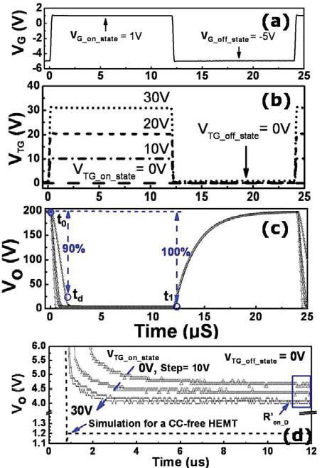
Figure 2: (a)–(c) Input pulse signals and drain output voltage (Vo) waveforms of DG-HEMT. (d) Drain output voltage (Vo) waveforms of DG-HEMT in on-state pulse mode. The on-state top-gate voltage (VTG_ON_state) is biased from 0V to 30V. The off-state top-gate voltage (VTG_OFF_state) is constantly biased at 0V. Dynamic Vo waveform simulation of current-collapse-free AlGaN/GaN HEMT based on DC characteristics.
The devices were tested over a 25μsec cycle with the device on and off 50% of the time (Figure 2). With +30V top-gate bias in the on-state, the falling delay time (τfd) was improved by 55% and the dynamic on-resistance (RON_D) by 17% compared with 0V top-gate bias (Table 1). With 0V top-gate, the setup mimics the effect of a source field-plate.
Table 1: Falling delay time (τfd) and dynamic on-resistance (RON_D) versus on-state top-gate voltage.
| VTG_ON_state (V) | τfd (μsec) | RON_D (Ω) |
| 0 | 1.6 | 500 |
| 10 | 0.94 | 460 |
| 20 | 0.78 | 430 |
| 30 | 0.72 | 415 |
However, the researchers estimate that without current collapse τfd could be as low as 0.56μsec, based on parasitic characteristics derived from static DC measurements. The 30V top-gate result is 29% longer than this. In addition, the static on-resistance of 115Ω is around a factor of three smaller than the best dynamic value.
Given that the top-gate bias would be expected to increase the carrier density in the two-dimensional electron gas (2DEG) channel by about 0.8x10¹³/cm2, the researchers believe that part of the current collapse effect involves the region between the top-gate and drain.
By comparing the dynamic on-resistance just before the switch to the off-state with the top-gate potential, the researchers estimate the intrinsic dynamic resistances below the top-gate (Rd1) and between the top-gate and drain contact (Rd2) to be 80Ω and 330Ω, respectively. The corresponding sheet resistances are 2000Ω/square and 4125Ω/square.
The higher sheet resistance of the d2 region suggests that the ‘current collapse’ there is not impacted by lateral current injection. Possible reasons could be hot-electron injection from the channel, or charges being trapped in the buffer layer, but the researchers write that the situation is not clear.
The researchers conclude from their study that current collapse under the top-gate (d1) affects more strongly the falling delay time while the d2 current collapse tends to reduce the dynamic on-resistance.
http://ieeexplore.ieee.org/xpl/login.jsp?tp=&arnumber=6515605
http://dx.doi.org/10.1109/LED.2013.2259213
The author Mike Cooke is a freelance technology journalist who has worked in the semiconductor and advanced technology sectors since 1997.
