


- News
12 July 2013
Self-terminating recess etch produces nitride transistor with +3V threshold
Peking and Xidian universities have jointly developed a self-terminating gate recess etch that allows them to produce aluminium gallium nitride (AlGaN) normally-off metal-oxide-semiconductor field-effect transistors (MOSFETs) with positive thresholds of up to +3.2V [Zhe Xu et al, IEEE Electron Device Letters, vol34, p855, 2013]. The maximum drain current of the device was more than 200mA/mm.
Nitride semiconductor transistors are of interest in high-frequency and high-power applications such as power switching, due to the high critical electrical field for breakdown. However, the devices tend to be normally-on, which leads to more complex circuits and increases power consumption. Also, in power applications one prefers the fail-safe operation of normally-off devices. One technique that pushes threshold voltages in a positive direction is gate recessing.
The Peking/Xidian devices used a GaN/Al0.3Ga0.7N/AlN/GaN (1nm/21nm/1nm/1.5μm) epiwafer produced on sapphire with metal-organic chemical vapor deposition (MOCVD). The wafer was found to have an electron sheet density of 8x10¹²/cm2 with mobility 1300cm2/V-s.
Device isolation was achieved using an inductively coupled plasma (ICP) mesa etch. The ohmic source-drain contacts consisted of titanium/aluminium/nickel/gold, rapid thermal annealed at 880°C for 30 seconds.
The gate recess process was enabled by a silicon dioxide mask, applied using plasma-enhanced chemical vapor deposition (PECVD). The gate region was defined by optical lithography and the mask was opened with another plasma-etch process. This open region was subjected to thermal oxidation at 615°C for 40 minutes, followed by etching with a potassium hydroxide solution at 70°C for 45 minutes.
The gate stack consisted of a 29nm atomic-layer deposited and annealed aluminium oxide (Al2O3) insulator, and a 3.5μm-long nickel/gold electrode. The gate width was 80μm. The source-drain, gate-source and gate-drain distances were 7.5μm, 1.5μm and 2.5μm, respectively.
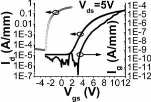 Figure 1: Log-scale transfer curve and gate leakage of fabricated device (solid lines) compared with log-scale transfer curve of conventional HEMT (dashed line).
Atomic force microscopy of the etched gate recess showed a root-mean-square roughness of 0.3nm, similar to that of the original AlGaN surface. The depth of the recess was 22.5nm, close to that of the AlGaN barrier 21nm +GaN cap (1nm) and AlN interlayer (1nm). The researchers say that these results, and others with variations in process conditions, “show that the recess etching process could be self-terminated at the AlGaN/GaN interface”.
The threshold voltage of the device was +3.2V, a high enough value to reliably operate despite switching noise. The maximum drain current density was 202mA/mm and the peak transconductance was 33mS/mm (Figure 1). The off-state drain current leakage was 10μA/mm. The gate leakage at 12V gate potential was 0.03mA/mm.
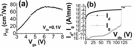
Figure 2: (a) Field-effect mobility and (b) breakdown voltage.
The maximum field-effect mobility was 75cm2/V-s, comparable with that of previously reported normally-off GaN-based MOSFETs, according to the team (Figure 2). The off-state (0V gate) breakdown (1mA/mm) occurred at 125V drain bias in a device with 3.5μm gate-drain distance. The researchers say that this is 60% higher than the value obtained for conventional HEMTs with a negative threshold voltage of -3V (75V for -5V gate off-state). The limiting factor for the breakdown voltage was the gate dielectric, leading to increased leakage.
The author Mike Cooke is a freelance technology journalist who has worked in the semiconductor and advanced technology sectors since 1997.
