
- News
25 July 2013
Combining Al2O3 and SiO2 for nitride semiconductor LED passivation
Researchers in China have developed a silicon dioxide (SiO2) on aluminium oxide (Al2O3) passivation for nitride semiconductor light-emitting diodes (LEDs) that offers more than two orders of magnitude reduced current leakage under reverse bias [Hao Guo et al, Appl. Phys. Express, vol6, p072103, 2013]. Further, by patterning the SiO2 layer with an array of hemispheres, the light output power (LOP) is increased by up to 22% at 60mA.
The research was based at Chinese Academy of Sciences’ Institute of Microelectronics, Southeast University, and Nanchang University.
The epitaxial material was grown using metal-organic chemical vapor deposition (MOCVD) on patterned sapphire. The pattern of 2.1μm diameter, 0.9μm height and 0.9μm separation was created using photolithography and inductively coupled plasma (ICP) etch.
The LED nitride semiconductor layers consisted of a 30nm GaN buffer, 4.5μm n-GaN contact, six-pair InGaN/GaN multi-quantum-well active region, and 0.9μm p-GaN contact. These layers were followed by 240nm of indium tin oxide (ITO) as a transparent conducting layer on the p-contact. Chromium/platinium/gold metal layers for the electrodes were deposited on the n-GaN and ITO. The devices emitted at wavelengths of around 460nm. The fabricated LED devices measured 300μm x 700μm.
After experimenting with various Al2O3, silicon nitride and SiO2 passivation layers for the LED, the researchers decided to develop a combined SiO2/ Al2O3 oxide process. The Al2O3 was found to have a good surface passivation effect, as evidenced by a very low reverse bias (-5V) leakage current of -9.3x10⁻¹⁰A when applied using atomic layer deposition (ALD). The surface passivation offered by plasma-enhanced chemical vapor deposited (PECVD) SiO2 was relatively poor, with a reverse bias leakage of -1.8x10⁻⁷A. However, the light output power (LOP) from the LED was 45.4mW with SiO2 passivation, compared with 42.7mW for the Al2O3 layer.
The effect of the Al2O3 passivation is believed to be a decreased trap density near the surface. Such surface traps provide routes for reverse leakage currents and for non-radiative surface recombination.
In the combined SiO2/Al2O3 passivation (Figure 1), the top SiO2 was also patterned into a triangular array of 2μm-diameter hemispheres spaced by 1μm, designed to reduce total internal reflection and hence increase light extraction. The Al2O3 layer was 10nm and the SiO2 500nm.
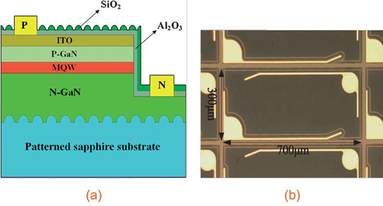
Figure 1: (a) Schematic of LED on patterned sapphire with patterned SiO2/Al2O3 passivation. (b) Photograph of fabricated 300μm x 700μm LED chips.
The hemispheres were formed by photolithography into a soft resist, which was then transferred into the SiO2 via inductively coupled plasma etch. The hemispherical shape was achieved by reflowing the patterned photoresist, i.e. the photoresist is melted and the surface tension of the liquid pulls the material into hemispherical shapes. By varying the reflow time and temperature, different diameters and heights could be achieved (Table 1).
| Sample | Reflow temperature (°C) | Reflow time (min) | Hemisphere height (nm) | Hemisphere base diameter (μm) |
| A | 0 | 0 | 491 | 1.56 |
| B | 160 | 5 | 476 | 1.58 |
| C | 160 | 7 | 456 | 1.63 |
| D | 160 | 9 | 347 | 1.69 |
| E | 160 | 11 | 205 | 1.86 |
Table 1: Measured surface etching profiles of patterned SiO2/Al2O3 passivation layer under different reflow conditions.
The resulting LEDs had very similar current-voltage characteristics. At 60mA, the forward voltage was 3.1V for all six devices.
However, the light output from sample D was greatest (Figure 2): at 60mA, the LOP for samples A-E were, respectively, 49.2mW, 52.9mW, 53.5mW, 55.2mW, and 50.9mW. A reference device with conventional SiO2 passivation had an LOP at the same current of 45.4mW. The sample D value of 55.2mW was 21.6% greater than that of the reference.
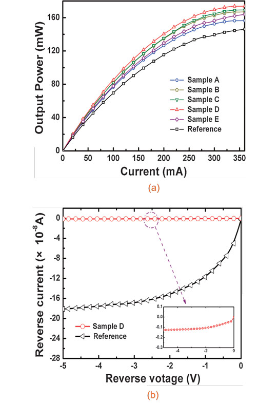
Figure 2: (a) LOP of fabricated LEDs as function of injection current. (b) Reverse leakage current characteristics of sample D and reference.
Another reflection of the improved performance with Al2O3 was increased electrostatic discharge resilience under 2000V reverse voltage stress that yielded 93.67% functioning devices for sample D, compared with 82.69% for the reference device.
Silicon dioxide on aluminium oxide passivation GaN LEDs MOCVD ICP etch
http://apex.jsap.jp/link?APEX/6/072103
The author Mike Cooke is a freelance technology journalist who has worked in the semiconductor and advanced technology sectors since 1997.