

- News
1 February 2013
Gated anode Schottky barrier diode enables increased forward current
Researchers in Korea have used aluminium gallium nitride (AlGaN) heterostructures similar to high-electron-mobility transistors (HEMTs) to create Schottky barrier diodes (SBDs) with increased forward current without damaging the breakdown performance [Jae-Gil Lee et al, IEEE Electron Device Letters, vol. 34, p.214, 2013, published online 16 January 2013]. The team was based at Hongik and Seoul National universities.
Schottky barrier diodes are used in many power switching applications such as switch mode power supplies (SMPS), converters, and inverters. It is hoped that nitride semiconductor based devices could use superior material properties such as high critical electric field and mobility values to boost performance in terms of breakdown voltage and switching speed.
The researchers used an epitaxial structure grown on a p-type silicon (111) substrate (Figure 1). The buffer conisisted of 3-4μm of GaN on a transition layer. This was followed by a 200Å Al0.25Ga0.75N barrier and a 12.5Å GaN cap.
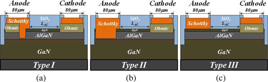
Figure 1: Cross-sectional schematics of AlGaN/GaN-on-Si rectifiers. (a) Rectifier with gated ohmic anode (type I), (b) recessed SBD (type II), and (c) conventional SBD (type III). Both anode and cathode contact areas are 80μm x 100μm. Type I has a 3μm-wide recessed region. The distance from the recessed edge to the Schottky overhang edge is 2μm in types I and II.
The rectifier with a gated ohmic anode was processed in a similar way to HEMTs with recessed gate, but with the gate and source being on top of each other (Figure 1a).
The Schottky contact of the ‘gate’ was recessed to leave 50Å between the electrode and two-dimensional electron gas (2DEG) channel. This was to ensure complete depletion of the 2DEG under the ‘gated-anode’ Schottky barrier. Without depletion, the device would operate as a resistor without rectifying capability.
The SBD structure was achieved with inductively coupled plasma reactive ion etching (ICP-RIE) for mesa isolation, silicon/titanium/aluminium/molybdenum/gold ohmic contacts annealed at 830°C for 30 seconds in nitrogen, more ICP-RIE for recessing, nickel/gold for the Schottky contact, and a 280nm silicon dioxide surface passivation.
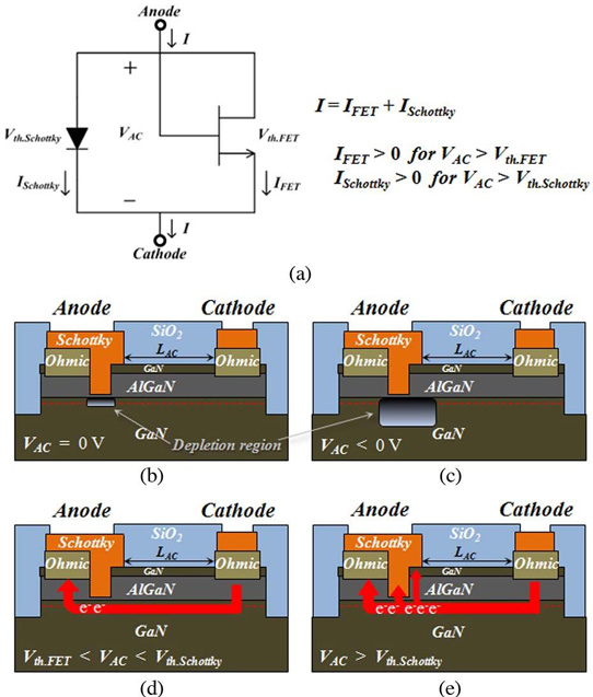
Figure 2: (a) Circuit model and operation mechanism of AlGaN/GaN rectifier with a gated ohmic anode. (b) Zero bias (VAC = 0V), (c) reverse bias (VAC < 0V), (d) small forward bias (Vth.FET < VAC < Vth.Schottky), and (e) large forward bias (VAC > Vth.Schottky) conditions. Vth.FET: Turn-on voltage of FET; Vth.Schottky: turn-on voltage of the Schottky diode.
The researchers see their device as being a combination of Schottky diode and normally-off FET (Figure 2). The effect of the combination is to lower the turn-on voltage without affecting the breakdown voltage characteristics (Table 1). Also, the forward current at 1.5V was 2-3x that of a conventional SBD (i.e. the type III device of Figure 1c).
| LAC μm) | Characteristics | Type I | Type II | Type III |
5 |
Vth (V) | 0.37 | 0.58 | 1.05 |
| VBD (V) | 489 | 467 | 483 | |
| IF (mA/mm) | 168.4 | 150.0 | 70.9 | |
| IR μA/mm) | 2 | 12 | 6.2 | |
8 |
Vth (V) | 0.38 | 0.58 | 1.05 |
| VBD (V) | 801 | 778 | 791 | |
| IF (mA/mm) | 133.3 | 118.0 | 53.6 | |
| IR μA/mm) | 3.2 | 8.2 | 5.4 | |
13 |
Vth (V) | 0.38 | 0.57 | 1.06 |
| VBD (V) | 1122 | 1120 | 1148 | |
| IF (mA/mm) | 108.2 | 89.1 | 39.5 | |
| IR (μA/mm) | 2.7 | 16 | 9.5 | |
18 |
Vth (V) | 0.37 | 0.57 | 1.06 |
| VBD (V) | 1440 | 1472 | 1451 | |
| IF (mA/mm) | 92.2 | 71.3 | 32.5 | |
| IR (μA/mm) | 2.2 | 20 | 16 |
Table 1. Device characteristics of different types.
Vth: turn-on voltage (current density 1mA/mm)
VBD: average breakdown voltage (leakage current 1mA/mm)
IF: forward current density (at 1.5V)
IR: reverse leakage current density (at 100V)
The researchers compared their device to one with a forward current of ~70mA/mm, turn-on voltage of 0.2V, and breakdown of 390V. This device was reported by Hong Kong University of Science and Technology in 2008. This earlier diode was also based on a nitride HEMT structure with an anode-cathode distance (LAC) of 10μm. Rather than recessing the gate, a fluorine plasma treatment was used to achieve normally-off behavior.
Schottky barrier diodes AlGaN GaN
http://ieeexplore.ieee.org/xpl/articleDetails.jsp?tp=&arnumber=6413168
The author Mike Cooke is a freelance technology journalist who has worked in the semiconductor and advanced technology sectors since 1997.
