


- News
9 December 2013
Growing high-quality free-standing GaN-on-silicon substrates
Researchers at Samsung Electronics and Seoul National University (SNU) in Korea have produced high-quality free-standing gallium nitride (GaN) substrates from hydride vapor phase epitaxy (HVPE) on silicon [Moonsang Lee et al, Appl. Phys. Express, vol6, p125502, 2013]. The main difference with normal attempts to grow free-standing GaN on silicon is that, instead of waiting for the material to cool, the researchers separated the GaN from the silicon substrate at high temperature.
Growing high-quality GaN on silicon should lead to larger-diameter wafers and therefore economies of scale in mass production. Although the experimental work was carried out on 2-inch silicon wafers, the researchers believe that production on 8-inch diameter substrates should be possible in the near future.
HVPE on silicon usually produces inferior free-standing GaN compared with material grown on sapphire, for example. This is due to the larger lattice mismatch between GaN and silicon of 16.9%. A further problem comes from different rates of thermal expansion: 5.59x10⁻⁶/K for GaN and 3.37x10⁻⁶/K for silicon. GaN is usually grown at high temperature and then separated at room temperature to give a free-standing wafer. As the material cools to room temperature on silicon, the different rates of contraction lead to cracks and bowing of the wafer.
Simulations suggest that, while the mismatch with silicon causes tensile stress in GaN at room temperature, above 900°C the GaN layer experiences mild compression. The researchers therefore believe that removing the silicon at high temperature could avoid the cracking and defect problems often found in producing free-standing GaN.
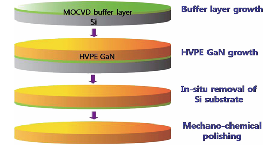
Figure 1: Schematic process steps for fabricating free-standing GaN-on-Si substrate using in-situ Si etching.
In the Samsung/SNU method, the 2-inch (111) silicon wafer is first cleaned to remove oxygen and to give a hydrogen-terminated surface. Buffer and transition layers are grown using metal-organic chemical vapor deposition (MOCVD).
The buffer consisted of 100nm of aluminium nitride (AlN). This layer reduces lattice mismatch and prevents silicon from diffusing from the substrate into the nitride semiconductor layers – an effect known as ‘melt-back’ that inhibits GaN growth.
The transition layer was a series of aluminium gallium nitride (AlGaN) layers with a “unique epitaxial structure” developed by Samsung along with researchers from Sejong and Hanyang universities [http://proceedings.spiedigitallibrary.org/]. The structure is designed to reduce dislocations and compensate for stress during growth.
The MOCVD processing was completed with a 500nm gallium nitride (GaN) layer (250arcsec x-ray rocking curve).
The HVPE of 400μm of GaN was carried out in a chamber that was also capable of in-situ etching. The HVPE process consisted of pre-reacting hydrogen chloride (HCl) with Ga liquid to form GaCl gas. The gas was transported to the growth zone at 1000°C to react with ammonia (NH3) to give GaN deposition on the MOCVD template. Nitrogen was used as a carrier gas for the HVPE. The growth rate of HVPE is much higher than for MOCVD, allowing thicker layers to develop.
The process was completed by etching away the silicon substrate at 1000°C using HCl gas. The reactor was then cooled to room temperature to yield the free-standing GaN. Microscopic inspection of the product showed an absence of cracks or defects such as melt-back and pits.
The (0002) x-ray rocking curve gave a peak with full-width at half maximum (FWHM) of 65arcsec for the Ga face and 200arcsec for the N-face. The difference is attributed to bowing and the fact that the N face comes from material at the junction with the MOCVD template layers. However, the amount of bowing is much reduced at about 20μm, compared with the hundreds of microns typical for free-standing GaN produced on foreign substrates that are removed at room temperature.
The estimated pit density after 30 minutes etching in phosphoric acid (H3PO4) was less than 106/cm2 over the whole wafer. This value is comparable to or better than that for thicker material (~1mm) grown on sapphire. Low etch pit densities (EPDs) indicate reduced numbers of dislocations.
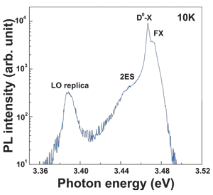 Figure 2: Photoluminescence spectrum of Samsung/SNU free-standing GaN at 10K: FX is attributed to free exciton; D0–X is neutral donor bound-exciton; 2ES is second excited state; LO replica is longitudinal optical phonon replica.
Photoluminescence at 10K (Figure 2) showed an edge peak close to that of free-standing GaN produced on sapphire. The researchers see their photoluminescence results as confirming the high crystal quality. However, the neutral donor bound-exciton (DBE) transition (D0–X) at 3.467eV (FWHM 3.1meV) is slightly red-shifted compared with strain-free ammonothermal GaN or material from homoepitaxy. The researchers see the red-shift as indicating slight tensile stress in their free-standing GaN from residual strain due to the quality difference of the Ga-face and N-face surfaces.
GaN-on-silicon substrates GaN HVPE
http://apex.jsap.jp/link?APEX/6/125502/
The author Mike Cooke is a freelance technology journalist who has worked in the semiconductor and advanced technology sectors since 1997.


