


- News
12 December 2013
Eulitha unveils litho system for photonic patterning
Eulitha AG (a spin-off of the Paul Scherrer Institute in Villigen, Switzerland that develops nano-lithographic technologies for optoelectronics, photonics, biotechnology and data storage applications) has announced the availability of the PhableR 100 photolithography system for printing high-resolution nano-structures, especially R&D applications as well as pilot and low-volume production. The system particularly targets the production of periodic patterns such as gratings and photonic crystals required in optics and photonics.
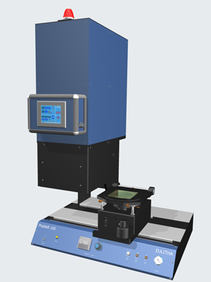 Picture: Eulitha’s new PhableR 100 system.
The PhablerR 100 system is based on the proprietary PHABLE (Photonics Enabler) photolithographic technology developed by Eulitha, which enables printing of high-resolution structures in a non-contact, proximity photolithography system. The resolution obtained with the PhableR 100 is essentially the same as what is obtainable from a deep-ultraviolet (DUV) projection lithography system, claims Eulitha, but without the complex and expensive optics and mechanics of such a system. For example, linear gratings with a half-pitch of 150nm can be printed with high uniformity. Also, the “practically unlimited” depth of focus of the image formed by the PhableR 100 means that the high-resolution patterns can be printed with high uniformity even onto non-flat substrates (which are commonly encountered in photonics applications).
The system can expose substrates with diameters up to 100mm using industry-standard chrome-on-glass or phase-shifting masks. The mask and the substrate are loaded manually onto the system and the exposure process is controlled by an onboard computer. Standard i-line photoresists (both positive and negative tone), which are available from common vendors, can be used. Linear or curved gratings, 2D photonic-crystal-type patterns with hexagonal or square symmetry can be printed with feature periods of less than 300nm. The system can also be used like a standard mask-aligner in either proximity or contact mode in order to print micron-scale structures. Targeted applications include R&D projects in photonics, fabrication of gratings for optical diffraction and spectroscopy, light extraction patterns on LEDs, patterned sapphire substrates and color filters.
“We are proud to introduce a solution that will enable our customers to perform high-resolution photolithography with a low-cost system for the first time,” says CEO Harun Solak. “This equipment is a result of a long-term development effort at both the Paul Scherrer Institut and Eulitha,” he adds. The system is available for immediate demonstration at the Eulitha site in Switzerland. The PhableR 100 also will be presented at the 13th International Nanotechnology Exhibition & Conference (nano tech 2014) at Tokyo Big Sight, Japan (29-31 January).
EVG collaborating with Eulitha on low-cost nanopatterning for HB-LEDs
Eulitha unveils PHABLE UV litho technology for photonics patterning
Eulitha Nanopatterning HB-LEDs


