


- News
18 December 2013
Evanescent wave coupling to increase light extraction efficiency
Researchers at the National Institute of Advanced Industrial Science and Technology (AIST) in Japan have used evanescent wave coupling to enhance the light output power of red light-emitting diodes (LEDs) by a factor of 3.8 [Guo-Dong Hao and Xue-Lun Wang, Appl. Phys. Lett., vol103, p231112, 2013]. The researchers comment: “We believe that our technique represents a significant step in the development of ultrahigh-efficiency LEDs.”
Guo-Dong Hao and Xue-Lun Wang designed ridge structures (Figure 1) to generate evanescent near-field electromagnetic waves that propagate along the semiconductor-air interface to the sub-wavelength ridge top and there be transformed into light.
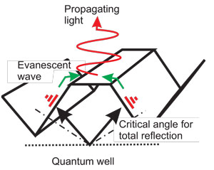 Figure 1: Evanescent wave coupling effect in sub-wavelength ridge structure.
Normal flat surface LEDs suffer from narrow escape cones where all light with an angle of incidence beyond some critical value is reflected back into the device, killing light extraction efficiency. The critical angle is controlled by the difference in refractive index between the LED and air.
The semiconductor structures for the AIST LEDs (Table 1) were grown on a 12mm x 13mm (001) gallium arsenide (GaAs) substrate by metal-organic vapor phase epitaxy (MOCVD). The substrate was misoriented 10degrees in the [110] direction to suppress spontaneous ordering of the alloyed compound semiconductor layers. Silicon (Si) and zinc (Zn) were used as doping for n- and p-type layers, respectively. The resulting wafer was annealed at 500°C for 2 minutes to activate the zinc doping.
Table 1: Epitaxial layers used for LEDs.
| Ohmic contact | p+-GaAs:Zn | 10nm |
| Current spreading | p-(Al0.7Ga0.3)0.5In0.5P:Zn | 2μm |
| Cladding | (Al0.7Ga0.3)0.5In0.5P | 0.2μm |
| Multiple quantum well | 3x((Al0.7Ga0.3)0.5In0.5P/Ga0.5In0.5P | Well ~ 7nm |
| Cladding | (Al0.7Ga0.3)0.5In0.5P | 0.1μm |
| Current spreading | n-(Al0.7Ga0.3)0.5In0.5P:Si | 2μm |
| Ridges | n-Al0.7Ga0.3As:Si | 0.8μm |
| Ohmic contact | n-GaAs:Si | 30nm |
| Etch stop | n-Al0.7Ga0.3As:Si | 0.4μm |
| Substrate | (001) GaAs |
The LED processing began with deposition of 1μm-diameter titanium/platinum/gold circular electrodes with 1% surface coverage on the p-GaAs ohmic contact layer. Further layers consisted of a silver (Ag) mirror, titanium/platinum diffusion barrier, and gold-tin eutectic bonding for flipping and attachment to an n-GaAs submount wafer with gold-germanium/nickel/gold ohmic contact layers on the back side and also a gold-tin eutectic bonding layer on the top. The eutectic layers were bonded at 380°C and 0.2MPa pressure.
The epitaxial growth substrate was removed by first milling down to 50μm and then wet etching the remaining material. The AlGaAs etch stop layer was removed with a different selective wet etch. A further wet etch was used with photolithography to create ridges for the evanescent wave coupling (Figure 2). The dimensions were chosen based on finite-difference time-domain simulation.
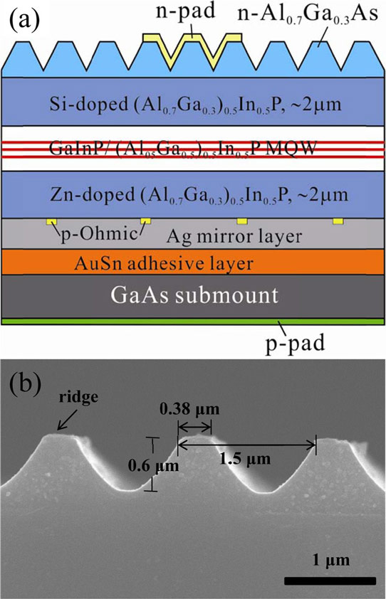
Figure 2: Schematic cross-section of AlGaInP LED with sub-wavelength ridge structure on light-extraction surface.
While the p-electrodes covered the entire back surface of the GaAs submount, the n-electrode (consisting of palladium/germanium/gold) was patterned into four whirlpool-shaped fingers covering about 4% of the n-contact surface. The resulting 1mm x 1mm LEDs were singulated with a final wet etch.
Two types of LED were produced from the same material: one type with ridges (R-LED) and the other without (F-LED). Current versus voltage measurements showed a series resistance that was higher for the R-LED (9Ω) than for the F-LED (4.5Ω). This was blamed on the smaller contact area of the R-LED (~1/4) and “suboptimal ohmic contact resistance”. The researchers report that they are working to optimize the contact resistance.
In terms of light output power (Figure 3), the ridges gave a 3.8x enhancement at low injection currents of ~5mA, but this factor reduced to ~3x at 100mA. The researchers point out that these enhancements are greater than that typically achieved using alternative techniques such as random surface roughening or photonic crystals (1.5-1.8x).
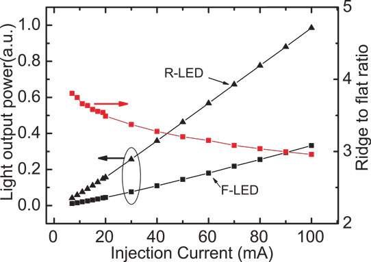
Figure 3: Comparison of measured light output power versus injection current (L-I) characteristics of F-RED and R-LED and enhancement ratio of the light output power of an R-LED compared to an F-LED.
The team attributes the more efficient light extraction of evanescent wave coupling to it not needing multiple reflections before radiation can emerge from the device. They comment: “A conventional AlGaInP-based LED requires at least 10 reflection events for light generated in its active layer to escape to the air even with an ideal diffuse surface.” Such a long light-path naturally leads to losses in the LED materials and at each reflection event.
The researchers explain the decline in enhancement at high current injection as being due to a faster decline in current-spreading efficiency for the device with ridges. Simulations suggest that the devices have a maximum current-spreading efficiency of 96% at low currents of 5mA. The flat F-LED current-spreading efficiency declines to 83% at 100mA, while the ridged R-LED’s efficiency degrades much faster to 64% at 100mA. Correcting the light output power enhancement factor for the current-spreading efficiency declines gives a steady performance of ~3.8x up to 100mA.
Red LEDs AlGaInP LEDs GaAs GaAs substrate MOCVD
http://dx.doi.org/10.1063/1.4842215
The author Mike Cooke is a freelance technology journalist who has worked in the semiconductor and advanced technology sectors since 1997.


