


- News
12 August 2013
Quantum dot lasers on silicon with stable operation at high temperature
University of Tokyo has improved the temperature performance of 1.3μm quantum dot (QD) laser diodes bonded to silicon [Katsuaki Tanabe et al, Appl. Phys. Express, vol6, p082703, 2013]. Photonic circuits are commonly created in silicon, but the light sources presently need to be produced using compound semiconductor technology.
In particular, researchers are seeking devices that are more stable over wide temperature ranges and that can operate at higher temperatures. The Tokyo devices used silicon-doping to provide partial p-type conduction in the gallium arsenide (GaAs) barriers around the self-assembled indium arsenide (InAs) QD that formed the active light-emitting regions of the laser diode devices. These devices were bonded onto silicon substrates.
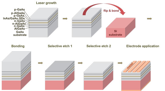
Figure 1. Schematic of fabrication of InAs/GaAs QD lasers on Si substrates.
The InAs/GaAs QDs were grown using molecular beam epitaxy (MBE) on GaAs substrate (Figure 1). The active region consisted of 8 layers of self-assembled InAs QDs in p-GaAs barriers. The dots had a per-layer density of 6x10¹⁰/cm2.
The AlGaAs n- and p-type cladding layers were 40% aluminium and 60% gallium. The 1μm AlGaAs etch stop on the GaAs substrate consisted of material with 70%-Al and 30%-Ga.
The QD material was flipped and bonded onto epi-ready p-Si (100) substrate. The QD material and substrate were first coated with photoresist and diced into 1cm2 dies. The purpose of the photoresist was to protect the interface between the QD structure and Si substrate from particles that could weaken the bond.
Two types of bonding process were tested: direct and metal-mediated. The direct wafer bonding was prepared for using a hydrofluoric acid dip to remove native oxide from the surfaces of the laser and substrate materials. The metal-mediated bonding consisted of coating the surfaces with 100nm of gold germanium nickel alloy applied using evaporation. The dies were bonded with their (110) edges aligned to facilitate cleavage of the laser facets. The bonded assembly was annealed at 300°C for 3 hours in air.
The removal of the GaAs substrate material was achieved by a two-stage wet etch in phosphoric acid-hydrogen peroxide and then citric acid-hydrogen peroxide. The edges of the wafer were coated with photoresist to avoid undercutting into the QD layers. The AlGaAs etch stop was removed with a hydrofluoric acid etch.
The material was used to create 2mm-cavity-length broad-area Fabry–Perot lasers with cleaved facets. The 100μm-wide laser stripes were coated top and bottom with gold/gold-germanium-nickel electrodes. The cleaved facets were not coated.
Both devices operate at more than 100°C with an emitted wavelength of 1.3μm (the O-band of optical communications). The researchers comment: “No significant difference in the temperature-dependent light–current characteristics is observed between the direct-bonded and metal-mediated-bonded QD lasers on Si substrates.”
The researchers compared the temperature performance of the new InAs/p-GaN QD lasers with that of devices without p-doping in the GaN barriers around the dots (Figure 2). The new p-doped devices had a higher characteristic T0 temperature (less variation of the threshold with temperature) due, it is thought, to “suppression of thermal excitation of holes in the lasing mode at higher temperatures”.
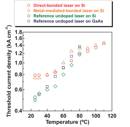
Figure 2. Temperature dependence of threshold current densities for p-doped and undoped 1.3μm InAs/GaAs QD lasers on Si and GaAs substrates.
The comparison devices were produced in previous work by the research team, and included a coating layer on the facets.
Around room temperature the T0 value for the p-doped LDs was effectively infinite (no change in threshold). One might note, however, that the room-temperature threshold was somewhat higher than for the undoped samples. Around 100°C, the T0 value was in the range 150-180K. The T0 for the comparison devices was around 60K across the whole temperature range.
“These lasing temperatures and T0 of our p-doped lasers are significantly higher than the cases of the previous works for telecommunication-band QW [quantum well] and QD lasers on silicon,” the researchers write, adding: “These results verify that III–V QD lasers on silicon fabricated by wafer bonding are promising for temperature-stable light sources in high-density photonic integrated circuits.”
http://apex.jsap.jp/link?APEX/6/082703/
The author Mike Cooke is a freelance technology journalist who has worked in the semiconductor and advanced technology sectors since 1997.
