


- News
29 August 2013
NTT uses LayTec’s EpiCurve TT to optimize InGaAs metamorphic buffer for laser diodes
LayTec AG of Berlin, Germany, which makes in-situ metrology systems for thin-film processes, focusing on compound semiconductor and photovoltaic applications, has announced that Ryo Nakao from NTT Photonics Laboratories (NTT) is using LayTec’s EpiCurve TT in-situ metrology system to improve layer thickness and indium content to fabricate a thin indium gallium arsenide (InGaAs) metamorphic buffer with low thermal resistance. Temperature characteristics of laser diodes (LDs) on GaAs substrate depend on the quality and the thermal resistance of InGaAs metamorphic buffer layer.
At the Electronic Materials Symposium (July 2013, Japan), NTT presented a new method for optimization of the metamorphic buffer layer for freestanding quasi-InGaAs substrates. LayTec’s in-situ tool helps understand the MOVPE growth conditions and shows the changes in wafer curvature caused by residual strain during MOVPE growth.
Figure 1 shows in-situ curvature data for a 1250nm metamorphic InGaAs buffer layer and a quasi-InGaAs substrate layer. The growth can be separated into three parts: 1) Coherent (pseudomorphic) growth of the buffer, 2) Growth with relaxation, 3) Free-standing (unstrained) growth. During relaxation, the in-plane lattice constant of the In0.12Ga0.88As layer increases. After the buffer has reached 1250nm, its lattice constant exactly matches the lattice constant of In0.10Ga0.90As. As a result, the wafer curvature does not change during the subsequent growth of In0.10Ga0.90As layer. The authors call this final growth phase ‘free-standing’ because the In0.10Ga0.90As layer grows with its natural lattice constant and creates a quasi-substrate similar to an In0.10Ga0.90As wafer for the later device growth.
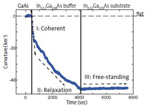 Figure 1: In-situ curvature data of InGaAs buffer and quasi-InGaAs substrate on GaAs substrate.
Further experiments with the same indium content and different buffer thicknesses showed that if the relaxation is not sufficient (buffer thickness=1000nm), the quasi- In0.10Ga0.90As substrate growth is compressively strained. However, over-relaxation (1600nm) results in a tensile strain.
The researchers plotted these changes to obtain a map of the correlation between thickness and curvature [1]. For a free-standing quasi-InGaAs substrate, they choose a buffer thickness with no further variation in curvature over time during In0.10Ga0.90As growth.
LayTec Metrology InGaAs Laser diodes
