


- News
1 August 2013
Gold-free CMOS-compatible nitride semiconductor Schottky barrier diodes
Researchers based in Belgium have developed gold-free nitride semiconductor Schottky barrier diodes (SBDs) on 200mm-diameter silicon to complement metal-insulator-semiconductor high-electron-mobility transistors (MISHEMTs) previously reported [Silvia Lenci et al, IEEE Electron Device Letters, published online 3 July 2013; MISHEMTs reported Imec processes first power devices on 200mm CMOS-compatible GaN-on-Si. The research team was based at imec, KULeuven and Ghent University.
Most nitride semiconductor devices use gold in the fabrication of Schottky and ohmic contacts. However, one would like to integrate such devices produced on silicon substrates with CMOS to benefit from the respective strengths, such as high breakdown in the nitride semiconductor section and unsurpassed CMOS logic performance. Gold is a killer of CMOS performance through its drastic reduction of carrier lifetimes in silicon.
The epitaxial structure of the SBD and MISHEMT devices (Figure 1) was obtained though metal-organic chemical vapor deposition (MOCVD) on 8-inch (200mm) <111> silicon. The aluminium gallium nitride (AlGaN) buffer was grown on a 200nm AlN nucleation layer. The buffer consisted of a series of steps down in Al-concentration: 400nm Al0.74Ga0.26N, 400nm Al0.44Ga0.56N, and 1800nm Al0.21Ga0.79N. This structure was then used as a template for the 150nm GaN channel and 15nm Al0.21Ga0.79N barrier. The wafer was capped with 2nm of GaN, and 140nm silicon nitride (SiN) passivation, applied using rapid thermal chemical vapor deposition (RTCVD).
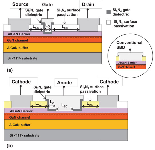
Figure 1: Schematic representation of (a) AlGaN-on-Si MISHEMT and (b) GET-SBD. Reference SBD is shown in circle.
Device isolation was achieved by nitrogen implantation. The anode and cathode regions of the Schottky barrier diode were opened using sulfur hexafluoride plasma etch of the passivation layer. The anode was further recessed by atomic layer etching of the barrier, leaving ~5nm AlGaN above the GaN channel.
The anode recess was lined with 15nm of RTCVD silicon nitride, which was also used as gate dielectric in the MISHEMT process. The silicon nitride was then etched to give an anode region with gate dielectric edge termination (GET). This was the only extra lithography step over the MISHEMT process. The use of GET aims to allow forward current flow across the Schottky contact length (LSC) while blocking reverse-bias flow leakage across the lateral shielding areas (LG).
The gold-free metal stack used for the Schottky anode contact and MISHEMT gate electrode consisted of 20nm of titanium nitride, 20nm of titanium, 250nm of aluminium, 20nm of titanium, and 60nm of titanium nitride. The gold-free cathode/source/drain ohmic metals were 20nm of titanium, 200nm of aluminium, 20nm of titanium, and 60nm of titanium nitride. The metals were annealed at 550°C.
Small diodes with single anode fingers of width 100μm were produced, along with multiple-finger diodes with a total width of 10mm. The anode-cathode distance was 10μm. The GET length (LG) was 1.5μm with the Schottky contact 6μm. The Schottky contact length for comparison conventional SBDs without GET was 9μm (1.5+6+1.5μm).
The forward current-voltage characteristic for the small GET-SBD was similar to the conventional SBD with the GET-SBD turning on a little faster. However, the reverse-bias current leakage was more than three orders of magnitude lower in the GET-SBD.
The researchers also studied the breakdown of GET-SBDs with different anode-cathode distances (Figure 2): with LAC of 5μm and 10μm, 1μA/mm breakdown occurred at -600V. Hard breakdown occurred at -800V for LAC of 10μm.
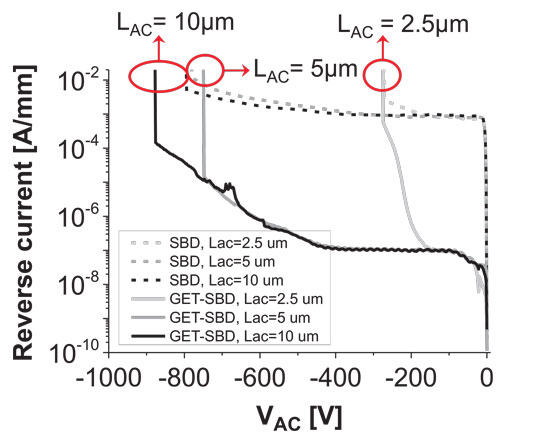
Figure 2: Reverse leakage current, measured until hard breakdown, of 100μm-wide rectifiers with varying anode-to-cathode spacing. Light gray, dark gray, and black curves: LAC = 2.5μm, 5μm, and 10μm, respectively. Solid lines: GET-SBDs. Dashed lines: conventional SBDs.
Although the reverse current leakage of the GET-SBD increases with temperature in the range 25-150°C, the researchers comment that the leakage is smaller at 150°C than in SBDs with gold-based electrodes at 130°C.
The larger multi-finger devices showed hard breakdown at -600V, “a symptom of possible epi-related defects across the wafer”. In the forward direction, these devices are capable of handling up to 2A current at 2V bias.
MISHEMTs produced on the same wafer demonstrated functionality with a negative (depletion-mode/normally-on) threshold voltage of -1V with a 10V drain bias. The hard breakdown voltages of these devices were higher than 600V.
The researchers comment: “When compared with Au-based AlGaN/GaN rectifiers, our Au-free devices had state-of-the-art turn-on and on-state voltages (0.41V and 1.14V, respectively), together with low reverse leakage current (within 1μA/mm at VAC = -600V).”
http://ieeexplore.ieee.org/xpl/articleDetails.jsp?arnumber=6553126
The author Mike Cooke is a freelance technology journalist who has worked in the semiconductor and advanced technology sectors since 1997.
