

- News
10 April 2013
High-speed modulation in high-power nitride semiconductor LEDs
Taiwan National Tsing Hua University has been studying ways to improve the modulation performance of high-output-power nitride semiconductor light-emitting diodes (LEDs) [Chien-Lan Liao et al, IEEE Electron Device Letters, published online 28 March 2013]. Up to now, most research effort for visible LEDs based on indium gallium nitride (InGaN) alloys has focused on extracting higher power efficiency for white light illumination and shorter-wavelength applications.
In principle, shorter-wavelength light should enable broader bandwidths for visible light over the normal infrared of fiber optical communication. With InGaN LEDs, high power output has generally resulted in poor modulation performance.
The Tsing Hua research has resulted in an InGaN LED with 225.4MHz 3dB-modulation bandwidth at 35mA injection current and 1.6mW output power. Previously high output power has resulted in modulation bandwidths of tens of MHz, although at lower output powers some groups have achieved 200-330MHz.
The researchers see their device as incorporating two key technologies: a gallium-doped zinc oxide (GZO) current-spreading layer and a smaller RC constant. The GZO transparent conducting oxide (TCO) layer creates a low contact resistance while also creating a uniform near-vertical current flow through the active light-emitting layers (Figure 1). The smaller RC constant is the result of employing smaller bonding pads and rapid thermal annealing to repair damage from plasma etch processes used in fabricating the device.
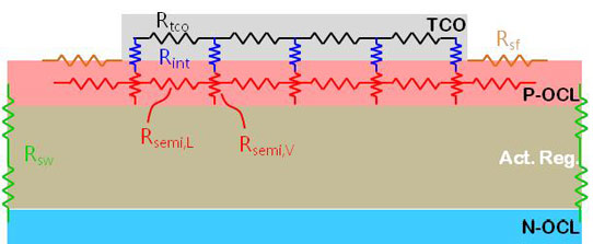
Figure 1: Resistivity optimization to create uniform near-vertical current flow through InGaN LED. This is achieved by minimizing the resistance of the TCO (Rtco), interface with (Rint) and the vertical component in the cap (Rsemi,V) of the ohmic contact layer (OCL), while maximizing the resistance of the surface (Rsf), MQW (Rsw) and lateral component for the cap (Rsemi,L).
The Tsing Hua LED wafer was grown using metal-organic chemical vapor deposition (MOCVD) on sapphire (Figure 2). The undoped GaN buffer layer was 800nm thick, the n+-GaN contact/confinement was 3000nm (3μm), the p-type aluminium gallium nitride (p-AlGaN) confinement was 20nm, the p-GaN cap was 560nm, and the n+-InGaN contact was 1.4nm. The multi-quantum well (MQW) light-emitting active region consisted of 5x 3nm InGaN wells separated by 4x 14.4nm GaN barriers.
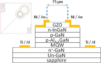 Figure 2: Epitaxial structure for blue high-speed LED. Inset: designed mask after overlapping with five steps.
The final 250nm GZO layer was applied using atomic layer deposition (ALD) with diethylzinc, triethylgallium, and water vapor precursors.
The LEDs were fabricated with ring electrodes to avoid excessive lateral current spreading. The current confined aperture was 75μm, with a 80μm-diameter bonding pad. The chip dimensions were 400μm x 400μm.
The sapphire substrate was lapped and polished from 430μm down to 130μm to improve its thermal conductance. Sapphire has a high thermal resistivity, which can cause problems with thermal management. Reducing the distance that heat has to cross sapphire was aimed at tackling this.
The peak wavelength of the device was ~441nm, although there was some blue-shift to shorter wavelengths at high current injection due to energy-level shifts in the MQW as electric fields are applied (the quantum-confined Stark effect). The capacitance of the device under reverse bias was low, at ~2pF on average. The capacitance of the bonding pad was also reduced by using relatively low-dielectric-constant silicon dioxide as insulator. The series resistance of the device was estimated to be 28Ω. The forward voltage at 20mA was 4.9V.
The researchers performed light output power and modulation bandwidth measurements (Figure 3). At 35mA, the power reached 1.6mW. The modulation bandwidth was measured as a 3dB reduction in output power (f3dB) compared with the DC performance (Figure 3 inset). The bandwidth increases with injection current level. At 35mA, a bandwidth of 225.4MHz was achieved.
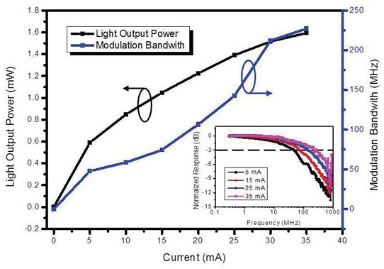
Figure 3: Light output power and 3dB frequency bandwidth (f3dB) as a function of forward current measured at 300K for 441nm high-speed LED. Inset: spectra of 3dB frequency bandwidth at various currents.
The researchers believe that further optimization of the confined region would increase the current density and hence the bandwidth. However there are trade-offs, since increased currents tend to heat devices, reducing efficiency, and there are also efficiency droop effects independent of self-heating (tested using pulsed operation). Efficiency droop has been ascribed to various causes such as Auger-type non-radiative recombination that kicks in at high current, polarization effects from the more ionic nature of the nitride semiconductor bond, and carriers overshooting the MQW light-emitting regions.
The author Mike Cooke is a freelance technology journalist who has worked in the semiconductor and advanced technology sectors since 1997.
