

- News
18 April 2013
Spectrolab expands from 100mm to 150mm solar cell wafers
Boeing Company subsidiary Spectrolab Inc of Sylmar, CA, USA has introduced 150mm-diameter germanium wafers into production (50mm larger than its prior 100mm wafers). The 50% increase in wafer diameter allows more than 2.5 times more gallium arsenide (GaAs) solar cells - or cells that are three times larger - to be grown on each wafer, reducing customers’ costs on solar cells by 10-25%, it is estimated.
 Picture:
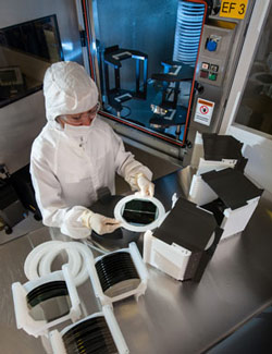
Spectrolab semiconductor processor Abraham Rizo inspects 150mm-diameter solar cell wafers.
Picture:
Spectrolab semiconductor processor Abraham Rizo inspects 150mm-diameter solar cell wafers.
For more than 55 years, Spectrolab has produced solar cells and panels for the space industry (powering satellites and interplanetary craft). Spectrolab became part of Boeing in 2000. For the past 10 years it has also produced ground-based concentrated photovoltaic (CPV) solar cells. In August 2009, Spectrolab set what was then a record for CPV solar cell energy conversion efficiency of 41.6%.
Now, to accommodate for the larger wafers, Spectrolab has modernized its factory to create a new 150mm solar cell wafer line. The upgrade, which involves re-purposing floor space previously used to produce silicon-based solar cells, also includes a new class 1000 cleanroom facility (requiring the use of full bunny suits) as well as material handling equipment.
A short video describing the wafer-size expansion and factory upgrade can be viewed at www.boeing.com/Features/.
