

- News
3 April 2013
Lowering tunneling resistance in GaN/InGaN/GaN structures
Ohio State University (OSU) has used polarization engineering to create low-resistance tunnel junctions in gallium nitride (GaN)-based structures [Sriram Krishnamoorthy et al, Appl. Phys. Lett., vol102, p113503, 2013]. Such junctions could be used to improve hole injection into light-emitting structures.
Normally, nitride semiconductor hole injection is achieved by creating p-type regions with magnesium-doping (Mg). Unfortunately, the Mg acceptor level is in the range 140-210meV above the valence band, meaning that the dopant concentration has to be high to achieve reasonable hole concentrations at room temperature (300K ~ 26meV).
By contrast, the silicon donor level for n-type doping is in the range 12-20meV below the conduction band. This makes low-resistance n-type conducting GaN relatively easy to achieve. In addition, even without doping, GaN has n-type characteristics due, it is thought, to electrons associated with nitrogen vacancies.
Tunnel junctions can be used to convert electrons from n-type regions into holes in thin p-type regions, improving injection into undoped active light-emitting regions. Without such structures, using a thick (200nm) p-GaN region as a hole source creates a relatively high-resistance volume of material and this tends to impede current spreading from metal electrodes.
Non-uniform current injection into light-emitting regions tends to reduce the power efficiency of electron-hole recombination into photons. On the other hand, increasing the metal electrode area to spread the current more evenly blocks light from emerging from the devices, lowering light extraction efficiency.
With tunnel junctions, the current could be spread more evenly in relatively low-resistance n-type regions and then converted to holes before injection into light-emitting structures.
Another possible application is producing devices where the p-injection region is under the n-type region. Presently, the p-region is grown last because of the difficulties in manufacture. It is thought that reversed-polarization quantum well LEDs could benefit from improved carrier injection and confinement. Also, multi-junction solar cells generally use tunnel junctions to connect different subcells in series.
Of course, this all depends on achieving tunnel junctions with relatively low resistance. The large bandgap of indium aluminium gallium nitride (InAlGaN) semiconductor materials would suggest low tunneling probabilities and high resistivity. However, these materials also have large spontaneous and strain-dependent (piezoelectric) electric polarizations that can lead to high electric fields in heterostructures.
OSU believes that these fields can be used to align the conduction and valence bands on opposite sides of a tunnel junction. The researchers carried out a number of theoretical investigations to provide guidelines for constructing junctions with high tunneling probability and low resistance.
A polarization-induced tunnel junction was then produced using nitrogen-plasma-assisted molecular beam epitaxy (PA-MBE) on nitrogen-face freestanding GaN templates (Figure 1a). The structure consisted of a pn junction with a tunnel junction feeding holes into the p-side. The 50μm x 50μm test device was created with titanium/gold ohmic metallization on the top n-contact, mesa isolation, and finally evaporation of metal on the bottom n-contact.
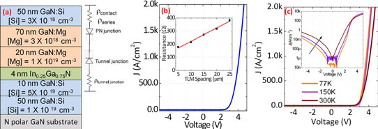
Figure 1: (a) Epitaxial stack of GaN p-n junction with GaN/InGaN/GaN tunneling contact layer to p-GaN. Circuit model shows two back-to-back diodes and various resistance components. (b) Characteristics of p-contactless p-n junction device showing negligible additional voltage drop across tunnel junction. Inset: resistance across transmission-line method pads with different spacing, used to extract specific top contact resistivity. (c) Temperature-dependent current-voltage (I-V) characteristics of device, showing efficient hole tunnel injection even at low temperatures. Inset: temperature-dependent I-V characteristics of device on logarithmic scale.
The structure demonstrated rectifying behavior (Figure 1b). The linear region of the forward bias region gives a series specific resistivity fit of 4.7x10⁻⁴Ω-cm2. The researchers estimate that the contribution of the top n-contact resistance was 3.5x10⁻⁴Ω-cm2, providing an upper limit on the specific resistivity of the tunnel junction of 1.2x10⁻⁴Ω-cm2. This is claimed as “the lowest observed resistance for a III-nitride tunnel junction”.
For a 100mA/cm2 current injection, the voltage drop across the pn junction is estimated at 3.05V and across the tunnel junction 12mV.
Temperature-dependent measurements show reduced current leakage under reverse bias at low temperature (Figure 1c). In addition, the forward current is maintained at the lower temperature of 77K. For a traditional nitride semiconductor pn junction one would expect the resistivity under forward bias to increase as the holes in the p-type region are frozen out of the system.
The researchers compared their results with a number of others in nitride and non-nitride material systems (Figure 2). They comment: “Although this device demonstration was performed on N-face orientation with the p-type layer down structure, similar characteristics would be obtained from a Ga-face n-GaN/InGaN tunnel junction on a +c-plane-oriented p-up p-n junction or LED structure. This implies that the low-resistance tunnel junctions demonstrated in this work can be directly extended to commercial c-plane LEDs.”
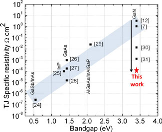 Figure 2: Tunnel junction resistivity in different material systems. The OSU structure demonstrates the lowest tunneling resistivity so far for GaN-based structure.
However, there remain some challenges such as activation of the buried p-type layer, particularly for devices grown using commercial metal-organic chemical vapor deposition (MOCVD). The researchers suggest activation through etched mesa sidewalls as a possible approach. Photon absorption losses in narrower-bandgap InGaN layers are also a concern for the demonstrated structure.
The researchers also believe that the polarization engineering of tunnel junctions could be applied to magnesium/zinc oxide devices, where p-type doping has been even more difficult to achieve than in nitride semiconductors.
The researchers received funding from US Office of Naval Research (ONR) under the DATE MURI program and the US National Science Foundation (NSF).
Tunnel junctions GaN LEDs PA-MBE
http://link.aip.org/link/doi/10.1063/1.4796041
The author Mike Cooke is a freelance technology journalist who has worked in the semiconductor and advanced technology sectors since 1997.
