

- News
27 September 2012
Silicon photonics market expected to triple in next 5 years
By blending optical technology with low-cost CMOS semiconductor processing, silicon photonics has tremendous potential as a new technology, according to market research firm Yole Développement in its new report ‘Silicon Photonics Market & Technologies'.
Silicon photonics is a disruptive technology that enables a new breed of monolithic optoelectronic devices, notes the firm. The goal is to deliver economic optical connectivity everywhere, from network level to intra-system level, and eventually chip-to-chip. Currently, except for the light source, all other optical functions (modulators, detection, waveguides, intelligence etc) can be embedded wafer-level at the silicon-on-insulator (SOI) substrate.
Yole notes that silicon photonics addresses different types of devices, such as:
- Individual components & subcomponents: used as a single-function silicon photonics device, e.g. variable optical attenuator (VOA), mux/demux, active filters and optical switches, or as optical engines combining optics and electronics.
- Transceiver-type products: embedded optical modules, transmitters/receivers, and active optical cables (AOCs).
- Future products: e.g. hybrid packaged devices and 3DICs/integrated optoelectronic chips.
Moreover, passive optical elements (such as arrayed waveguides, optical fi lters, couplers, splitters, polarizer arrays) can be created with silicon photonics technologies and integrated with active elements.
In the report, Yole distinguishes between silicon photonics, CMOS photonics, hybrid silicon photonics, and III-V integrated photonics.
For a long time, silicon photonics has been constrained to R&D labs, but the first products have now shipped and an industrial infrastructure has been established step-by-step, the firm adds.
Datacoms to dwarf all other applications
However, although silicon photonics can address a wide range of applications, very few firms are actually shipping products.
The potential markets are:
- Telecoms - metro and long-haul applications;
- Datacoms - data centers and campus applications;
- Consumer - connecting desktop PC devices and PCs with HDTVs;
- High-performance computing (HPC) & data centers - using AOCs or embedded modules;
- Professional/commercial video - digital signage, digital cinemas, video recording and studios;
- Metrology and sensors - measurement of time, temperature, sound, frequency, stress and range using special silicon photonics sensors;
- Medical - DNA, glucose, molecular and cellular analysis etc, using special silicon photonics sensors;
- Military/aerospace/scientific - scientific instruments at corporate and national labs (aircraft, space missile, radar, imaging, and intelligence applications).
Data communications is the biggest market and will dwarf all other silicon photonics applications, reckons Yole. Indeed, major datacom protocols are all moving to high-speed signaling and surpassing 10Gbps, where reach and signal integrity issues are surfacing for both copper and optical technologies. There is a clear trend to surpass 25Gb in datacom protocols, and this is where silicon photonics will make sense, says the firm.
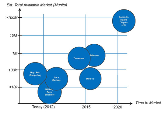
Figure 1: Total addressable market (TAM) for silicon photonics applications.
Demand will be driven by the need for: low-cost, high-speed interconnects supporting ever-increasing data rates at and beyond 25Gbps; and reach distance/data rates not served by vertical-cavity surface-emitting lasers (VCSELs).
Challenges ahead
However, silicon photonics still faces big industrial and technical challenges, says Yole:
• few products currently exist;
• few companies have developed integrated product solutions;
• costs are high;
• CAE/CAD programs are almost non-existent;
• technical mismatches exist;
• there is competition with VCSEL-based alternatives; and
• high volumes are needed.
For several years now, silicon photonics projects have been under the umbrella of large-scale R&D projects to set up roadmaps, says Yole. But now, multi-wafer project (MPW) service foundries are opening, and more industrial foundry activities are being established.
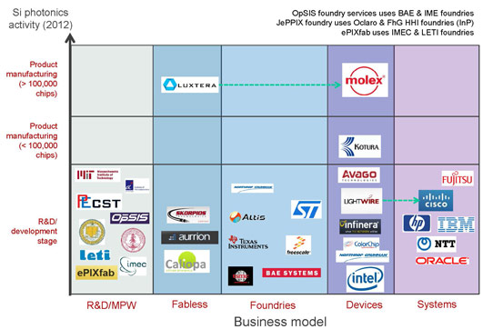
Figure 2: Map of silicon photonics players.
However, generic technologies and production platforms are needed to achieve low cost/high volume. As the future lies in the separation of design and fabrication, the silicon photonics sector is seeking an electronics-like foundry model. The map of players involved in silicon photonics already shows a significant number of foundry services, says Yole.
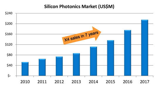
Figure 3: Silicon photonics market forecast.
Although the industry is trying to use as much as possible of the existing CMOS processes, 3D-ICs technologies will contribute to silicon photonics, especially regarding wafer bonding and 3D interconnects, the firm reckons.
Although the market is expected to grow by a factor of three in the next five years, the business could explode after 2020, as inter- and intra-chip communications could make this market grow by a factor of 10, concludes Yole.