- News
17 September 2012
Arsenide nanowires on graphite and graphene
Researchers at Norwegian University of Science and Technology (NTNU) have succeeded in growing gallium arsenide (GaAs) and indium arsenide (InAs) compound semiconductor crystal nanowires (NWs) on graphitic substrates such as few-layer graphene [A. Mazid Munshi et al, Nano Lett., published online 13 August 2012]. The researchers see this as a breakthrough, since earlier attempts to grow semiconductor crystal thin films on graphene and other graphitic substrates have thus far failed.
The NTNU spin-out Crayonano AS has already patented the technology developed by a team under the leadership of the company’s founders, NTNU professors Helge Weman and Bjørn-Ove Fimland.
“We do not see this as a new product,” Weman says. “This is a template for a new production method for semiconductor devices. We expect solar cells and light-emitting diodes to be first in line when future applications are planned.”
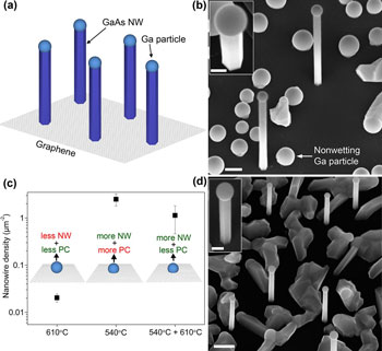 Figure 1: (a) Schematic of self-catalyzed GaAs nanowires on graphitic surface. (b) SEM image of nanowires grown on graphite. Inset, near top-view image. (c) Variation in average nanowire density with growth temperature. Insets: schematic of contact angles of Ga catalyst droplet at different temperatures. (d) SEM image of nanowires grown on graphite by two-temperature growth. Inset: tilted-view image of one nanowire. Scale bars are 200nm in the main figures and 100nm in insets.
Crayonano sees application potential for self-powered nanomachines and advanced 3D integrated circuits built on graphene and semiconductor nanowires, enabling smaller and more efficient electronics with self-powered consumer devices integrated into everything from clothes to notepads, along with more traditional uses in cell phones, tablets and exercise accessories.
The paper adds: “We anticipate this particular GaAs nanowire/graphene hybrid to be promising for flexible and low-cost solar cells.”
The researchers also analyzed the ways in which compound semiconductor crystals can accommodate themselves to the underlying graphite/graphene hexagonal chickenwire structure. They found that their grown material fitted well with their theoretical concepts. In particular, growth of nanowires accommodates a larger mismatch in lattice parameters, compared with thin films of semiconductor.
The vertical GaAs nanowires (Figure 2) were grown on graphitic and few-layer graphene surfaces using self-catalyzed vapor-liquid-solid molecular beam epitaxy (MBE). The flux of the source gases needs to be optimized to increase the number of nanowires (NWs) and decrease the occurrence of parasitic crystals (PCs). In particular, it was found that a reduced temperature of 540°C was needed in the nucleation phase to form GaAs droplets with reduced contact angle that seems to favor the growth of nanowires. The nucleation was followed by a higher-temperature growth step at 610°C that reduced the number of PCs. The nucleation phase lasted 10 seconds and the higher-temperature growth step was five minutes long.
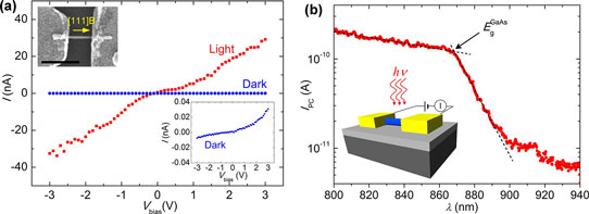
Figure 2: Photocurrent response of a single GaAs nanowire photodetector. (a) I−V curves of a single GaAs nanowire photodetector. Blue circles are measured dark current; red squares are measured photocurrent. Photocurrent was measured using an 800nm laser line with estimated power density of ~2.5kW/cm2. Bottom inset: dark current with enlarged y-axis. Top inset: SEM image of photodetector. Scale bar 500nm. (b) Wavelength dependence of photocurrent for nanowire at applied bias of 50mV. From crossing of black dashed lines, absorption edge was estimated to be ~869nm (1.427eV), denoted by black arrow. Inset: schematic of fabricated nanowire photodetector.
The graphene-based nanowires were grown on graphene produced through epitaxy on silicon carbide (SiC) substrates. The researchers have also grown InAs NWs on graphite.
High-resolution transmission electron micrography (HR-TEM) showed zincblende (ZB) and wurzite (WZ) crystal structure sections of the NWs, with ZB predominant. However, in the lower sections a mixture of segments are found that the researchers attribute to “a combination of catalyst droplet shape change due to the two-temperature transition and strain relaxation in the nanowire due to the growth on a lattice-mismatched substrate”.
The researchers says that there is a need to control the nucleation introduced by external manipulation to allow increased nanowire density and further reduction of parasitic crystallites. Ultimately, they want to find a method for positioning the vertical semiconductor nanowires on graphene for device applications, rather than depending on random initiation of the NW growth.
The researchers used GaAs NWs produced on graphite to create photodetectors (Figure 2). The contacts consisted of gold. In dark-mode, the resistance was more than 1G. With laser illumination, the current increases by three orders of magnitude. Due to the high surface charge density of the unpassivated NWs, the researchers believe that the majority of the photocurrent arises from the metal-semiconductor contact region. The calculated responsitivity is ~30mA/W, “which is three orders of magnitude larger than previously reported for a single GaAs nanowire.”
The good optoelectronic performance of these devices is taken as an indication of the high purity of the wires with no apparent contamination from the graphite substrate. A sharp absorption edge occurs at a wavelength around 869nm with a width of about 30nm (50meV), which is comparable to the performance of intrinsic crystalline GaAs.
The researchers conclude: “These results convey that GaAs nanowires grown on graphite are at least of similar optoelectronic quality as the ones grown on GaAs substrates, and hence can be equally useful for nanowire optoelectronic applications.”
GaAs nanowires InAs nanowires Graphitic substrates Graphene SiC substrates Solar cells LEDs
The author Mike Cooke is a freelance technology journalist who has worked in the semiconductor and advanced technology sectors since 1997.