

- News
9 October 2012
Reducing nitride LED droop with AlInN superlattice electron blocking
University of California, Santa Barbara has reduced efficiency droop while maintaining peak efficiency in nitride semiconductor light-emitting diodes (LEDs) through the use of an aluminium indium nitride (AlInN) superlattice (SL) for electron blocking [Roy B. Chung et al, Appl. Phys. Lett., vol101, p131113, 2012].
Nitride semiconductor LEDs suffer from large efficiency droop at high current. One source of this effect is thought to be from electrons overshooting the active light-emitting region, ending up in the p-contact layers. These electrons generally recombine with holes non-radiatively. This both wastes the electron and reduces hole injection into the active region.
To combat this effect, aluminium gallium nitride (AlGaN) electron-blocking layers (EBLs) are often used. Unfortunately, these barriers not only keep the electrons in the active region, they also impede hole injection.
One unpleasant factor of AlGaN layers is that they are subject to tensile strain due to lattice mismatch with the underlying GaN crystal structure. Such strain tends to lead to material quality degradation and reduced performance for LEDs. By contrast, AlInN with indium content around 18% matches the GaN crystal structure parameters and could lead to better-performing EBLs. In addition, the valence band offset (or hole barrier) is smaller than with AlGaN. However, AlInN growth is relatively immature and there is still a large amount of development work needed to optimize and find the limitations of the material.
The researchers used metal-organic chemical vapor deposition (MOCVD) on sapphire in a Veeco P-75 vertical reactor. To create LEDs, various p-doping processes for the AlInN layers were explored. The active region consisted of six InGaN quantum wells and barriers (Figure 1). The electron-blocking layer consisted of either a single lattice-matched (18% In) AlInN layer or a sequence of AlInN/GaN layers making up a superlattice. A conventional AlGaN EBL was also produced for comparison. The magnesium (Mg) doping of the superlattice layers was heavier for AlInN than for GaN.
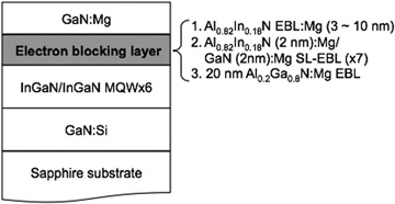 Figure 1: Schematic diagram of LED structure with various EBLs.
The material was used to make 200µm x 500µm LEDs with a tin-doped indium tin oxide (ITO) transparent conducting layer p-electrode and a titanium/aluminum/nickel/gold n-electrode. The devices were mounted on silver headers and encapsulated.
One problem with a single AlInN EBL is that the layer is quite resistive, and under high Mg-doping the crystal quality deteriorates. The material also has an oxygen incorporation of around 1018/cm2, which leads to the donation of electrons and hence could be a factor reducing the hole carrier density through compensation. With increased thickness of AlInN EBL, the operating voltage increases and the light output power decreases at a current injection of 20mA. Neither of these effects is desirable.
The researchers believe that the structural degradation by Mg doping and the compensation effect by the unintentional donor impurity have the strongest impacts on LED performance, compared with other possibilities.
The superlattice structure, by contrast, showed similar light output power compared with the LED that had a conventional AlGaN EBL. The power at 20mA was 23.8mW for the SL LED and 24.76mW for the AlGaN LED. The injection current was pulsed with a 1% duty cycle to avoid self-heating effects.
The SL LED further showed improved current droop performance over the AlGaN LED (Figure 2a). The peak external quantum efficiency (EQE) was 42% for the SL EBL and 43% for the AlGaN EBL. While the SL EBL device continued with little change in EQE up to 100A/cm2 current density, the AlGaN EBL LED began to droop at 50A/cm2. At 300A/cm2, the droop from the peak was 17% with an SL EBL, but 36% with an AlGaN EBL.
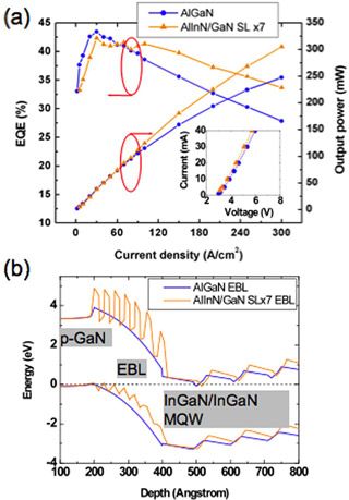 Figure 2: (a) EQE and light output power as a function of current density for LEDs with SL EBL (orange triangles) and AlGaN EBL (blue circles), with inset showing current–voltage characteristics of LEDs (DC operation), and (b) calculated band diagram comparison between AlGaN and AlInN/GaN SL EBL structures.
The operating voltage at 20mA was 4.4V with SL EBL and 4.6V with AlGaN EBL. These relatively high operating voltages are attributed to “unoptimized ITO process and p-GaN, resulting in the high contact resistance”.
The measured valence-band offset between lattice-matched AlInN and GaN is 0.2–0.3eV, giving a 0.7–0.8eV conduction-band offset. In the SL structure, the conduction-band offset has an extra 0.4eV compared with the AlGaN value. The researchers think that this could explain the delay in droop performance. Simulations (Figure 2b) suggest that the repeated thin layers of AlInN of the SL could also minimize tunneling effects while avoiding structural degradation caused by doping. The slight reduction in the simulated hole barrier would improve hole transport into the active region.
Thermal droop improved in semi-polar nitride semiconductor LEDs
Layer insertion to avoid nitride LED efficiency droop
LED droop LEDs AlInN AlGan EBLs
http://link.aip.org/link/doi/10.1063/1.4756791
The author Mike Cooke is a freelance technology journalist who has worked in the semiconductor and advanced technology sectors since 1997.