

- News
7 November 2012
In-situ silane treatment enhances light output from nitride LEDs
National Chung Hsing University in Taiwan has developed a simple silane treatment to improve crystal quality/internal quantum efficiency (IQE) and light extraction in nitride semiconductor light-emitting diodes (LEDs) [Chung-Chieh Yang et al, IEEE Electron Device Letters, published online 16 October 2012].
The treatment creates air voids between the buffer and n-type contact of the LED material. The air voids block threading dislocations from the buffer from reaching the active light-emitting region. Also the air voids scatter the light produced, allowing light trapped by reflection at flat gallium nitride/air boundaries to escape.
The nitride semiconductor layers (Figure 1d) were grown on c-plane patterned sapphire substrates using metal-organic chemical vapor deposition (MOCVD). Growth began with 30nm of 550°C gallium nitride (GaN) nucleation, followed by 2µm 1150°C undoped u-GaN buffer.
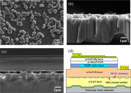
Figure 1: (a) Bird’s-eye view at 45° and (b) cross-sectional SEM micrographs of u-GaN layer with random 3D island structure. (c) Series of air-voids in re-grown LED structure. (d) Schematic diagram of SA-LED.
Before further growth, the surface was treated with silane (SiH4) at 950°C, producing air-voids in the subsequent 3µm n-GaN layer (Figure 1c). The silane treatment for 20 minutes created a random silicon nitride (SiNx) passivation layer. The voids began as the gaps between a series of 3D islands of 950°C n-GaN grown vertically for 10 minutes on the unpassivated areas of the u-GaN buffer. The height of the islands was around 0.9µm (Figures 1a and b).
A second silane treatment was then made to prevent further growth on the sidewalls of the islands. During the treatment the temperature was ramped up to 1180°C. Further n-GaN was then grown on the island base that coalesced in a manner rather similar to epitaxial lateral overgrowth (ELOG), but without using a mask. The researchers refer to their ‘series-of-air-voids’ (SEAV) process as being an in-situ ELOG process. The air-voids form in the spaces between the islands (Figure 1c).
X-ray diffraction and etch-pit analyses of the n-GaN material showed improved quality with silane treatment. The diffraction peaks for the (002) and (102) planes of material with silane treatment had rocking curve full-widths-at-half-maximum (FWHM) of 280 arcsec and 225 arsec, respectively. The corresponding values for material grown without the silane treatment were 405 arcsec and 340 arcsec, indicating lower crystalline quality.
The etch-pit densities were 7.6x10⁷/cm2 with silane treatment and almost an order of magnitude larger at 6.5x10⁸/cm2 without. Low etch-pit densities are associated with lower amounts of threading dislocations (TDs) and defects that reduce LED performance.
The researchers conclude that the SEAV process “acted as a TD-stopping structure to reduce the defect density in the SA-LED structure.”
The indium gallium nitride active region consisted of a 9-period In0.2Ga0.8N/In0.01Ga0.99N (3nm/13nm) multi-quantum well (MQW). The electron-blocking layer was also a superlattice (of aluminium gallium nitride) with a 6-period p-type Al0.3Ga0.7N/GaN (2nm/2nm) structure. The p-contact layer was 0.13µm of p-GaN.
Along with the SEAV LED (SA-LED), a comparison standard nitride semiconductor LED device (ST-LED), without the silane treatment, was also produced.
The epitaxial material was processed into LEDs with 250nm of indium tin oxide (ITO) transparent conductor on the p-contact, and chromium/gold (Cr/Au) n- and p-type metal contacts.
The SEAV LED showed a 68% enhancement in light output at 20mA compared with the standard LED (Figure 2). The enhancement was attributed to both improved quality of the epitaxial material and light scattering encouraged by the air-voids that increases light extraction over that obtained from flat surfaces, which suffer from light trapping due to the small escape cone of the GaN–air interface.
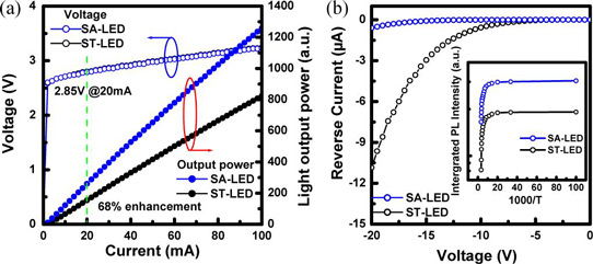
Figure 2: (a) Light output powers and operating voltages for ST-LED and SA-LED with varying injection current. (b) Reverse-bias current vs voltage (I–V) characteristics of ST-LED and SA-LED. Inset: IQEs of both LEDs measured through temperature-dependent PL.
The peak wavelength at 20mA was 443nm and the forward voltage was 2.85V, with similar values for the standard device. The leakage current under –10V reverse bias was lower for the SEAV device at 3.6x10⁻⁹A, compared with 5.7x10⁻⁷A for the standard LED. The lower reverse bias current is another indication of the lower defect densities of the SEAV epitaxial material.
Photoluminescence experiments showed an internal quantum efficiency (IQE) for the SEAV material of 54.6% at room temperature (300K), relative to the 10K value. The corresponding figure for the standard material was 42.4%.
The angular distribution of the emitted light was also affected by the presence of air-voids, giving a narrower divergence for the SEAV LED.
LEDs GaN Silicon nitride MOCVD Threading dislocations
http://ieeexplore.ieee.org/xpl/articleDetails.jsp?tp=&arnumber=6331507
The author Mike Cooke is a freelance technology journalist who has worked in the semiconductor and advanced technology sectors since 1997.