- News
12 November 2012
Gold-doped graphene for transparent current spreading in UV LEDs
Researchers in Korea have developed gold-doped graphene as a transparent and current-spreading electrode (TCSE) for ultraviolet (UV) light-emitting diodes (LEDs) [Tae Hoon Seo et al, Appl. Phys. Express, vol5, p115101, 2012].
Some of the research group from Chonbuk National University and Sungkyungkyun University last year reported with others on the use of monolayer graphene for transparent conduction in nitride semiconductor UV LEDs [Developing monolayer graphene for transparent conduction in nitride semiconductor LEDs].
One problem with using graphene as a TCSE is high sheet resistance. Recently, another group in Korea has used gold nanoparticles to improve graphene performance as TCSE in nitride semiconductor LEDs [Boosting transparent conduction in graphene with gold nanoparticles].
Suggested applications for near UV (300–400nm) include germicidal instrumentation, biological agent identification, chemical sensing, fluorescence excitation, and optical data storage. Further, UV can be used as a pumping source for creating white light through phosphorescence.
An alternative technology for TCSEs is indium tin oxide (ITO), which provides low sheet resistances. However, as the wavelength enters the UV region, ITO’s transparency to light is severely curtailed.
The aluminium indium gallium nitride (AlInGaN) semiconductor material for the 380nm UV LED was grown using metal-organic chemical vapor deposition (MOCVD) on sapphire (Figure 1). Mesa regions were formed in the material by inductively coupled plasma (ICP) etch down to the n-type layers.
Contact |
p-GaN |
1040°C |
100nm |
Electron blocking |
p-AlGaN (Al 25%) |
1040°C |
25nm |
Multi-quantum well |
5xInGaN/AlGaN (In 4%, Al 8%) |
800°C |
2nm/12nm |
Contact |
n-GaN |
1040°C |
2μm |
Buffer |
GaN |
1040°C |
1.5μm |
Nucleation/buffer |
GaN |
550°C |
30nm |
Substrate |
Sapphire |
|
|
Figure 1: Epitaxial material structure of UV LED.
The graphene was produced through chemical vapor deposition (CVD) on 70μm copper foil and then transferred to the UV LED. Gold trichloride (AuCl3) in nitromethane was spin coated on the graphene layer on the UV LED. The optimum gold doping was obtained with a 10mM AuCl3 concentration. The graphene TCSE structure that was used was a bilayer with an interlayer distance of 0.38nm.
Annealing of the assembly was carried out for 30 minutes at 500°C to prevent oxidation of the LED and to strengthen the adhesion between graphene and p-GaN contact.
The metal electrodes for both the p- and n-contacts consisted of chromium and gold layers. A conventional LED with ITO transparent conducting layer was also produced.
The gold doping was found to have a slight effect on transmittance. At a wavelength of 380nm, the transmittance of undoped ‘pristine’ graphene was 92% and the transmittance of gold-doped graphene was 88.5%. A comparison 200nm ITO layer had transmittance of 74%. The wavelength dependence of the graphene films was small, but the ITO only showed reasonable transmittance in the visible-infrared range of 400nm to 800nm.
The researchers comment: “The loss in optical transmittance of the graphene film after Au doping was about 3.5% owing to Au nanoparticles acting as a scattering center for the light.”
 The advantage of the gold doping was seen in the much lower sheet resistance of 90Ω/square, compared with 500Ω/square for the undoped graphene layer. UV photoelectron spectroscopy (UPS) revealed another effect of gold doping – a shift in work function from 4.51eV for undoped graphene to 4.90eV for the doped layer. ITO has been measured with similar techniques as having a work function of ~4.5eV.
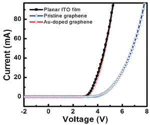
Figure 2: Current–voltage (I–V) curves for InGaN/AlGaN UV LED with pristine graphene film, Au-doped graphene film, and conventional planar ITO layer.
The gold-doped graphene LED showed improved electrical performance and light output (Figures 2 and 3). The forward voltage at 20mA was 3.98V, compared with 5.85V for an LED with undoped graphene TCSE. The forward voltage was only slightly more than the 3.92V of the 200nm ITO TCSE. The high forward voltage of the undoped graphene is a reflection of the material’s higher sheet resistance, along with the larger work-function difference with that of p-GaN (5.5-5.9eV).
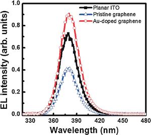
 Figure 3: Electroluminescence (EL) spectra at an applied current of 100mA of InGaN/AlGaN UV LED with pristine graphene film, Au-doped graphene film, and conventional planar ITO layer.
The emission from the gold-doped graphene LED was enhanced by about 20% over that of the ITO LED. Here, the improvement is related to the improved transmittance of graphene at the target wavelength, along with low work-function difference, while maintaining effective current spreading.
The researchers comment: “Further efficiency enhancement can be expected in GaN-based UV LEDs using graphene as their electrical properties are improved further.”
Developing monolayer graphene for transparent conduction in nitride semiconductor LEDs
Boosting transparent conduction in graphene with gold nanoparticles
UV LEDs Graphene AlInGaN MOCVD GaN Sapphire substrates
The author Mike Cooke is a freelance technology journalist who has worked in the semiconductor and advanced technology sectors since 1997.


