- News
15 May 2012
Nanoporous GaN for vertical LED lift-off
Yale University has developed techniques to release nitride semiconductor layers and transfer them to other substrates, allowing vertical current-flow light-emitting diodes (LEDs) [Yu Zhang et al, Appl. Phys. Lett., vol100, p181908, 2012].
The Yale technique creates a nanoporous (NP) layer of gallium nitride (GaN) using an electrochemical etch. Further nitride layers are then grown. A new substrate can then be applied to the top of the structure and the growth substrate removed at the weakened nanoporous region.
Nitride LEDs are grown commercially on sapphire substrates. However, sapphire is electrically and thermally insulating, which are not ideal properties for LEDs. With such devices both the contact pads are usually placed on the nitride layers and some of the current flow through the device is in a lateral direction, creating current bunching effects that reduce efficiency.
Vertical current flow can be arranged by releasing the nitride layers from the growth substrate. Various techniques have been developed such as laser lift-off and under-etching. However, these techniques can be slow or expensive to implement in manufacturing.
In the Yale method, a silicon-doped n-GaN layer was first grown on sapphire using a standard two-step metal-organic chemical vapor deposition (MOCVD) process. The GaN layer was then subjected as the anode in an oxalic acid electrolyte to electrochemical etching with a platinum cathode. By controlling the electric potential, the porosity of the GaN can be varied from sparse narrow pores (10%) to electropolishing (>60%). The etching proceeds selectively near pore tips following electric field/current flow lines.
For epitaxial lift-off purposes (Figure 1a), the researchers used a two-step etch with a change in bias midway, giving a 300nm-thick high-porosity (>50%) layer capped with a 240nm low-porosity (~10%) layer.
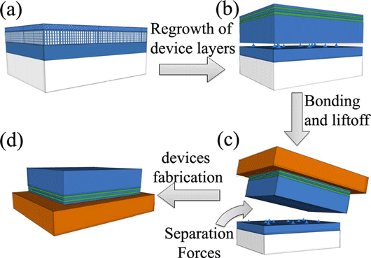
Figure 1: Conceptual process flow of epitaxial lift-off beginning from (a) preparation of GaN with designed porosity profile, (b) MOCVD overgrowth of GaN device layers and transformation of NP GaN into voided region for subsequent lift-off, (c) wafer bonding after GaN growth, and (d) room-temperature separation and layer transfer for thin-film vertical LED devices.
After cleaning, the wafers were subjected to further MOCVD of 5x InGaN/GaN multi-quantum wells between a 3μm n-GaN buffer and a 200nm p-GaN cap (Figure 1b). During the MOCVD process, the initial pores are transformed into air gaps. The overgrown material is tethered to the template by mesoscale pillars with a density of 105/cm2.
A large-area lift-off demonstration was performed by bonding a glass slide to the top with a two-part epoxy with a pressure of 30kPa. The lift-off was found to be crack-free. Also, the strain from growth on the lattice-mismatched substrate, measured using Raman spectroscopy, was fully relaxed upon separation by lift-off.
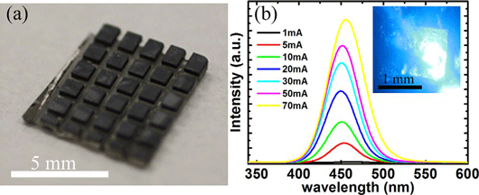
Figure 2: (a) Image of diced, 1mm-square InGaN LED thin films bonded to p-Si wafer and (b) room-temperature electroluminescence spectra and optical image at 5mA current injection of vertical LED from lift-off process.
The lift-off technique was also used to create vertical current-flow LEDs by bonding the epitaxial material to p-type silicon. The bond between the nitride and silicon semiconductors consisted of titanium/nickel p-contact metals and silver epoxy. The bonded wafers were diced into 1mm squares using a diamond saw. The sapphire substrate pieces were removed using tweezers. Preliminary electroluminescence spectra have been measured at room temperature (Figure 2).
GaN Vertical LED lift-off MOCVD
The author Mike Cooke is a freelance technology journalist who has worked in the semiconductor and advanced technology sectors since 1997.