- News
8 May 2012
NGK’s GaN substrate yields HB-LED chip with 90% IQE at 200mA
NGK Insulators Ltd of Nagoya, Japan has developed gallium nitride (GaN) wafers that, it claims, double the luminous efficiency of an LED light source compared with conventional materials.
 Grown using original liquid phase epitaxial (LPE) technology, NGK's GaN wafer (which was exhibited at SEMICON Japan last December) has shown low defect density and colorless transparency over the whole wafer surface.
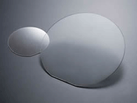
Image (right): GaN substrates (left: 2 inches, right: 4 inches).
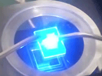
With the assistance of an external research institute, a light-emitting test was performed on an LED chip made using NGK’s GaN wafer. The test demonstrated an internal quantum efficiency (IQE) of 90% at an injection current of 200mA (compared with 30-40% for LED chips currently on the market). Luminous efficiency was 200lm/W, which is twice that using wafers currently on the market, it is reckoned. For the same brightness, this halves power consumption. Since the wafer reduces heat generation within LEDs, it can lengthen the lifetime of LEDs and enable the downsizing of lighting equipment, the firm claims.
 Earlier this month , NGK established the new department ‘Wafer Project’, aiming to speed the commercialization of wafer products. This year the firm aims to start shipping sample 4-inch-diameter GaN substrate, which is reckoned to be the world's first 4-inch GaN wafer produced using LPE growth technology.
Image (right): LED chip under light-emitting test: substrate size, 1cm square; chip size, 0.3mm square; injection current, 200mA; center wavelength, 450nm.
NGK is also accelerating its development of GaN wafers with lower defect density and larger diameters (6 inches), targeting applications such as power devices for hybrid cars, electric vehicles and power amplifiers for cellular base-stations. The firm reckons that GaN substrates are optimum for such applications, taking advantage of features such as high breakdown voltage and high frequency operation. HB-LEDs
NGK introduces LPE-grown GaN substrate for UHB-LED applications