- News
16 March 2012
First RF power operation report for AlGaN barrier HEMT on diamond
NTT Basic Research Laboratories in Japan has demonstrated “for the first time” RF power operation of aluminum gallium nitride (AlGaN) barrier high-electron-mobility transistors (HEMTs) epitaxially grown on diamond [Kazuyuki Hirama et al, IEEE ELECTRON DEVICE LETTERS, published online 2 March 2012].
The attraction of diamond as a substrate is the higher thermal conductivity (up to 22W/cm-K), allowing greater heat dissipation than alternatives such as sapphire (0.5W/cm-K), silicon (1.5W/cm-K), or even silicon carbide (4.0W/cm-K). Heat dissipation is particularly important in high output-power-density devices. Although molecular beam epitaxy (MBE) has previously been used to create nitride semiconductor HEMTs on diamond that demonstrated small-signal performance at 21GHz gain cut-off (fT), power operation and high breakdown voltage had not been reported until the new NTT work.
The NTT devices were grown on 5mm x 5mm 0.3mm-thick IIa-type diamond (111) substrates using metal-organic chemical vapor deposition (MOCVD) – see Figure 1. The ‘type’ represents the amount of nitrogen impurity in the diamond structure. For type IIa, the amount of nitrogen is less than 1016/cm3. Reducing the amount of nitrogen increases thermal conductivity: for type IIa, the thermal conductivity is more than 22W/cm-K, compared with 10-18W/cm-K for type Ib diamond (N concentration up to 3x10¹⁹/cm3).
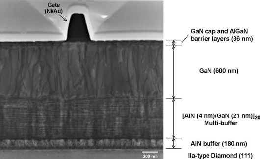
Figure 1: Cross-sectional bright-field TEM image of the AlGaN/GaN HEMT structure epitaxially grown on diamond (111) substrate. The multi-buffer region consists of 20 repeats of the structure shown. The 32nm AlGaN barrier had 33% aluminum content.
No passivation layer was applied to the HEMTs. The threading dislocation density in the thick GaN layer was estimated at 8.4x10⁹/cm2, which is comparable to the values for devices grown on sapphire substrates. X-ray diffraction analysis gave an estimate for (tensile) strain in the thick GaN layer of -0.01%. This low strain avoided crack formation.
The ohmic source/drain contacts consisted of titanium/aluminum/nickel/gold. The Schottky gate consisted of nickel/gold. The two-finger gate length was 0.4μm. The width was 100μm or 400μm. The source/drain separation was 5μm. The gate was placed centrally within the gap.
The maximum drain current was 770mA/mm and the off-state breakdown voltage at -6V gate potential (VBD) was 165V. The researchers comment: “This VBD is the highest ever reported for AlGaN/GaN HEMTs on diamond, and also comparable to VBD of typical AlGaN/GaN HEMTs with gate–drain spacing of about 2μm and without a field-plate structure.”
By halving both the maximum drain current and off-state breakdown voltage to give the bias points for A-class amplifier operation, the researchers estimate a potential output power density of 16W/mm.
The transconductance of 160mS/mm is lower than that achieved for devices produced on silicon carbide or silicon substrates. This is attributed to relatively low mobility of the two-dimensional electron gas (2DEG) channel (780cm2/V-s) and the relatively thick (36nm) barrier/cap layers.
Comparison with the DC performance showed little drain current collapse under pulsed operation, unlike with normal nitride semiconductor HEMTs. There was also less self-heating of the device.
The frequency performance showed a maximum available gain (fT) of only 25GHz, and maximum oscillation (fmax) of 18GHz. Nitride semiconductor HEMTs produced on other substrates have achieved hundreds of gigahertz values for these parameters. The researchers comment that the low transconductance impacts the frequency performance. Also, the use on a non-T gate would probably increase the gate resistance.
 A power sweep at 1GHz gave maximum output power of 2.13W/mm, maximum power gain of 28dB and power-added efficiency (PAE) of 46%. The bias point was 50mA drain current, 50V drain voltage, and -1.6V gate potential. The maximum output power fell short of the expected value of 3.13W/mm. This was attributed to impedance mismatch between the device and load of the testing system.
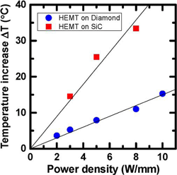
Figure 2: Power density dependence of temperature increase on diamond and silicon carbide.
The thermal performance of devices on diamond was compared with that of devices on silicon carbide, using infrared thermography (Figure 2). The thermal resistances derived from the slope of temperature increase with power density were 1.5K-mm/W for the diamond device and 4.2K-mm/W for the silicon carbide device. The type IIa diamond substrate also performed much better than a previously reported device on higher-nitrogen-content type Ib diamond that had a resistance of 4.1K-mm/W.
AlGaN/GaN HEMT Diamond substrates
The author Mike Cooke is a freelance technology journalist who has worked in the semiconductor and advanced technology sectors since 1997.