- News
15 March 2012
Watt-level QCL emission at 3.3μm without antimony
ETH-Zürich’s Institute for Quantum Electronics have produced short wavelength (3-4μm) quantum cascade laser (QCLs) without using antimony (Sb) as part of the material structure [A Bismuto et al, Semicond. Sci. Technol. vol27, p045013, 2012]. Watt-level emission was obtained at 3.3μm at room temperature, and pulsed operation lasing was achieved beyond 350K.
Using antimony in the lasing material has allowed QCLs to be created in this spectral range with low current threshold and low power consumption. However, the growth of aluminum gallium indium arsenide antimonide (AlGaInAsSb) combinations can be difficult to achieve using most processes developed for high performance laser operation.
Structures such as AlSb/GaAs/InAs/AlInSb on GaSb substrate have been used for short wavelength QCLs. The laser operation is continuous wave at room temperature, based on interband cascade transitions. However, these devices suffer from relatively low slope efficiencies and high thermal degradation, as represented by low characteristic temperatures (less than 50K for both threshold current and slope efficiency).
The researchers see QCL devices as potential coherent light sources for the mid-infrared “first atmospheric window” that falls in the 3-5μm range. A large number of gases can be detected through light absorption level such as methane, nitric oxide, carbon monoxide, carbon dioxide, formaldehyde, and so on. Further, stretching modes of C-H, N-H and O-H bonds fall in this range. These absorption levels can be several orders of magnitude larger than the overtone and combination bands that fall in the near infrared. The higher absorption should allow measurement of extremely low concentrations using simpler, more compact systems.
Other possible applications include metrology, industrial control and clinical diagnostic systems.
However, QCLs designed for this range of wavelengths suffer from a number of problems. Some of these are due to the electronic band structure of the usual compound semiconductor materials. Other problems include interface roughness and material strain control.
The ETH team has focused on developing a non-Sb system of strain-compensated layers of InGaAs/InAlAs on indium phosphide (InP) substrates. The thickness of the barriers and wells had to be tuned so that strain levels and band offsets could be maintained. The strains for AlAs barriers and In0.72Ga0.28As wells are +3.54% and -1.34%, respectively. These strain targets put constraints on the layer thicknesses. In this system, the AlAs thickness is restricted to about a third of that of the InGaAs well.
In order to ease these constraints, an InAlAs/AlAs composite barrier was developed. The growth process for InAlAs/AlAs (4.7nm/1.6nm) superlattices was first optimized, x-ray analysis suggesting that a growth temperature of 493°C was optimum. In fact, for the developed QCLs, the AlAs was restricted to less than 1nm to avoid excessive strain in the individual barriers due to the higher complexity of laser structures as opposed to simple superlattices.
The QCL structures were grown on InP substrates. X-ray analysis indicated that the strain was perfectly balanced between +3.5% compressive strain in the AlAs barriers and -1.3% tensile stress in the InGaAs wells. The overall strain was around 0.1%.
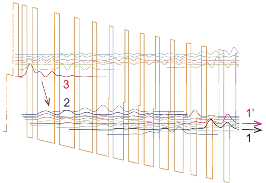
Figure 1: Conduction band diagram of one period of the active region at an average field of 120kV/cm. Calculated moduli squared of the relevant envelope wavefunctions are shown.
The active region of the device consisted of 30 period cascade repetitions (Figure 1) sandwiched between 200nm InGaAs confinement layers. Suitably doped cladding layers of InP and InGaAs were added. The material was formed into ridged waveguide laser diodes using wet chemical etching. Electrical insulation was provided by silicon dioxide. The top contact was titanium/platinum/gold. The device was thinned to 180μm before application of the bottom contact of germanium/gold/nickel/gold.
The researchers report on the performance: “Watt-level emission is observed at room temperature and the laser performance is comparable to what was observed for Sb-containing QCLs.” The characteristic temperatures for thermal degradation of threshold current and slope efficiency (increase in laser power output with current) are 70K (T0) and 100K (T1), respectively.
 Figure 2: Tuning behavior with corresponding peak optical output power of the external-cavity QCL at various wavelengths. Measurements were taken at 288K at a duty cycle of 1.5% (15ns, 1MHz) at different currents. Schematic sketch of external-cavity QCL setup operated in Littrow configuration.
With a Littrow external cavity, a 3mm-long 15μm-wide device produced single-mode emissions tunable in the range 3.15-3.4μm (Figure 2).
With a view to continuous wave performance, the researchers have also begun development of buried heterostructure (BH) QCLs. First-order distributed feedback gratings were defined using holography on the 200nm InGaAs confinement layer above the active region. The 80nm grating depth was wet etched. The grating was then buried in the n-InP cladding layer. Ridge widths were created between 3μm and 6μm, again using a wet etch. Lateral electrical insulation was supplied by iron-doped InP deposited on the side of the ridges.
These devices are not satisfactory as yet, although single mode emission is observed at 250K. The researchers found significant leakage current and ageing effects. The leakage problem is attributed to use of the BH structure and, in particular, high aluminum content material. Voids in the Fe-InP insulating layers are also observed. New etching processes are being developed to overcome this problem.
The researchers believe that careful optimization of the active region medium could open up the whole first atmospheric spectral region. One possible route to this could be through heterogeneous cascade structures.
Short-wavelength quantum cascade lasing without antimony
QCL InGaAs/InAlAs InP substrates
The author Mike Cooke is a freelance technology journalist who has worked in the semiconductor and advanced technology sectors since 1997.