- News
25 June 2012
Nitride LED transfer from silicon to copper increases light output by 122%
Researchers in China have transferred nitride semiconductor light-emitting diodes (LEDs) grown on silicon (Si) to copper submounts, giving a 122% increase in light output at 350mA injection current [Tufu Chen et al, Appl. Phys. Lett., vol100, p241112, 2012]. The research was carried out at Sun Yat-sen University’s State Key Laboratory of Optoelectronic Materials and Technologies.
Growth of nitride semiconductors on silicon is expected to lower costs due to access to larger-diameter wafer substrates, particular for power and high-frequency transistors. For LEDs, light absorption in the narrower-bandgap substrate material needs to be avoided, for example by interposing mirror layers.
Another technique is substrate removal, which can be achieved by transfer to a copper submount and thinning/etch. Copper is attractive for this application due to its good electrical and thermal conductivity.
Such techniques were proposed by Nagoya Institute of Technology in Japan in 2005, giving 49% more light than before substrate removal. In 2010, Hong Kong University of Science and Technology reported a 70% enhancement from the transfer of nitride LEDs to copper.
The Sun Yat-sen University researchers began by growing crack-free indium gallium nitride (InGaN) multi-quantum-well (MQW) layers on Si (111) substrates using metal-organic chemical vapor deposition (MOCVD).
A thin interlayer of GaN was grown at low pressure (70mbar) between high-temperature aluminum nitride (AlN) buffer and normal pressure (300mbar) GaN. The aim of the interlayer was to speed the transition between the 3D growth of the buffer and the 2D (‘island’) growth favored for thin high-quality layer LED structures. Low-temperature AlN interlayers were used to control stress in the preliminary epitaxial layers.
The further epitaxial structure consisted of 0.8μm undoped GaN, 0.75μm n-GaN (1050°C), 10-periods of 2nm-thick In0.12Ga0.88N MQWs with 17nm-thick GaN barriers (880°C), and ending with a 0.15μm p-GaN cap (1050°C).
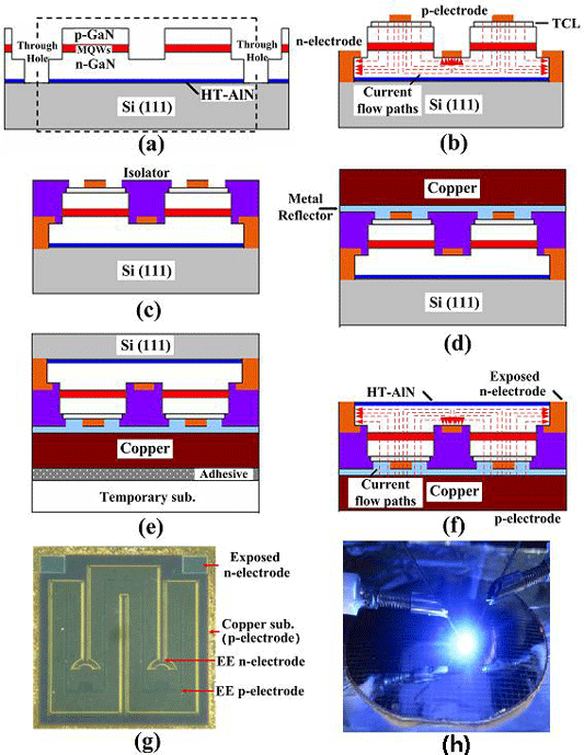
Figure 1: Fabrication process of LEDs on copper submount: (a) etch through-holes and the mesa by ICP-RIE, (b) deposit TCL and p/n electrodes, (c) isolate n-electrode and p-electrode, (d) deposit metal reflector onto exposed TCL surface, and electroplate 100μm-thick copper, (e) bond the wafer to a temporary substrate using acrylate adhesive and thin silicon substrate, (f) remove Si substrate by wet-chemical etching and separate from temporary substrate. (g) Photograph of 1mm x 1mm LED on copper. (h) Light-emitting image of LEDs on 2-inch electroplated copper submount at 350mA current injection. Current flow paths of conventional LED on Si and LED on copper are shown in (b) and (f), respectively.
The epitaxial material was prepared for transfer to the copper submount by drilling through-holes to the silicon substrate using inductively coupled plasma reactive ion etching (Figure 1a). Mesas were then formed, also using ICP-RIE. This was followed by thermal annealing at 700°C in nitrogen for 25 minutes to activate the p-GaN and partially repair plasma damage.
Then nickel/gold (5nm/7nm) layers were applied and annealed at 550°C for 15 minutes in air to form a p-type nickel oxide transparent conducting layer (TCL). Layers of chromium/aluminum/palladium/gold (Cr/Al/Pd/Au) were then added and annealed as p- and n-electrodes (Figure 1b). In this process, the through-holes were also filled with metal.
The different polarity electrodes were isolated with an insulating material (Figure 1c) and a Cr/Al/Pd/Au metal reflector and 100μm copper submount were applied (Figure 1d). The main reflecting component was Al; the gold was used as a seed layer for copper electroplating.
The electroplating technique is unaffected by the concave wafer bowing that occurs with nitride semiconductor layers on silicon. Bowing makes alternative wafer bonding methods difficult to implement.
The structure was flipped onto a temporary substrate to allow thinning of the silicon substrate down to 100μm (Figure 1e), prior to complete removal using a wet chemical etch with hydrofluoric-nitric-acetic (HNA) acid (Figure 1f). The n-electrodes consist of the metal-filled through-holes and the process thus avoids further need to etch the HT-AlN layer at this stage.
The forward voltage at 350mA current was 3.75V, a 0.4V increase on that of a conventional LED produced from the same epitaxial material. The researchers suggest that the increased forward voltage may be due to a poor interface between the p-GaN and the metal reflector. The forward voltage could be reduced by process optimization of the interface contact, the researchers believe.
The wavelength peak of the light (~450nm, blue) emitted by the LED on copper was blue-shifted by 5nm (i.e. to shorter wavelengths) compared with the conventional device. The researchers attribute this to strain relaxation of the crystal structure in the LED on copper, which was also found in x-ray diffraction measurements.
Nitride semiconductor devices have strong polarization fields, some of which arise from strain in lattice-mismatched structures (piezoelectricity). These fields tend to shift energy levels, and emissions are thereby shifted in the red/longer-wavelength direction. This is termed the quantum-confined Stark effect (QCSE). With lower strain, one expects less QCSE and higher internal quantum efficiency.
Another consequence of QCSE is shifts in peak emission wavelength as the applied field changes. With the LED on copper, there was no obvious wavelength shift as the injected current increased from 5mA to 300mA.
In terms of total emissions, the LED on copper showed a 122% increase over the conventional device at 350mA (Figure 2). The conventional device was produced as for the copper device up to Figure 1b. The improvement for the LED on copper was attributed to a number of factors: removal of the absorptive silicon substrate, elimination of electrode-shading losses, the rough AlN surface improving light extraction, and better thermal management with better heat conduction through copper than silicon.
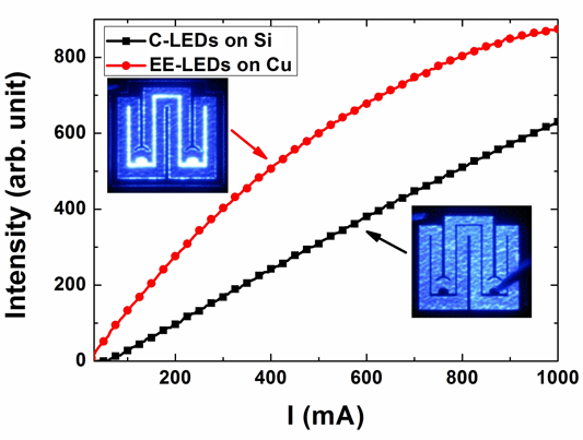
Figure 2: Light output versus current (L-I) characteristics of conventional LED on silicon and LED on copper. Light-emitting images of conventional LED on Si and LED on copper at 5mA current injection are shown in insets.
At higher currents, the light output with the LED on copper begins to saturate. This is attributed to the poor contact between the nickel oxide TCL and metal reflector that is thought to impede heat dissipation.
The insets in Figure 2 suggest significant current crowding for the LED on copper due to the poor contact between the metal reflector and TCL. The bright areas correspond to the thick metal p-electrodes. In the conventional LED, light emitted from these regions is blocked by the electrode, so the current crowding is not observed.
The author Mike Cooke is a freelance technology journalist who has worked in the semiconductor and advanced technology sectors since 1997.