- News
18 June 2012
Record 370GHz cut-off for InAlN barrier on GaN HEMT
University of Notre Dame (UND) and IQE RF LLC of Somerset, NJ, USA have achieved record cut-off frequencies of 370GHz for InAlN/AlN/GaN/SiC high-electron-mobility transistors (HEMTs) [Yuanzheng Yue et al, IEEE Electron Device Letters, published online 7 June 2012].
The use of indium aluminum nitride (InAlN) barrier layers rather than aluminum gallium nitride (AlGaN) allows lattice matching with GaN. In addition, a higher polarization discontinuity leads to higher charge density in the two-dimensional electron gas (2DEG) that forms in the GaN channel layer near the barrier/channel interface. The greater charge density allows for thinner barriers to be used, bringing the gate closer to the channel, improving electrostatic control.
In addition to use of the InAlN-based barrier layers, the UND/IQE team used dielectric-free passivation (DFP), rectangular gates and re-grown source–drain regions to improve performance through a reduction in the effects of parasitic passive resistance and capacitance.
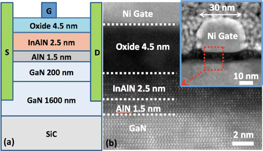
Figure 1: (a) Schematic of the InAlN/AlN/GaN HEMT cross section and (b) high-resolution TEM and (inset) scanning TEM images confirming HEMT layer structures and 30nm gate length after device fabrication.
The epitaxial structures were grown on silicon carbide using metal-organic chemical vapor deposition (MOCVD) — see Figure 1. The 1.6μm GaN buffer layer was iron-doped (Fe) to increase its resistivity, hence reducing the amount of current leakage through the buffer. A 200nm unintentionally doped GaN layer was followed by an AlN spacer and In0.17G0.83N barrier that is lattice matched to GaN.
Silicon dioxide was used as a mask layer for etch and molecular beam epitaxy (MBE) of the source–drain regions. The separation between the 40nm-deep source–drain wells was 865nm. The source–drain material consisted of silicon-doped n-GaN, grown to a height of 80nm. Polycrystalline GaN was removed from the oxide with a buffer hydrofluoric acid lift-off process. Ohmic source–drain contacts were made to non-alloyed titanium/aluminum layers. This was followed by mesa isolation using a chlorine plasma etch.
The dielectric-free passivation consisted of oxygen plasma treatment that oxidizes about 4.5nm of the original ~7.5nm InAlN barrier. Rectangular nickel gates were applied with a length of 30nm and a width of 2x25μm.
The maximum drain current of the resulting device was 1.5A/mm at zero gate potential and 5V drain. The on-resistance was 0.78Ω-mm between drain biases of 0 and 0.5V. The researchers find a difference 0.24Ω-mm, with the sum of the source and drain resistances (0.54Ω-mm) calculated on the basis of four-probe transmission line model (TLM) measurements. The origin of the difference is said to be unclear.
Pulsed measurements showed a slightly higher drain current at zero gate potential due to the suppression of self-heating. Nitride HEMTs often suffer ‘current collapse’ under such pulsed conditions. Although the device does not show current collapse, there is a 6% drain lag, “which merits further investigation”.
The peak intrinsic transconductance was 650mS/mm at drain bias 3V and drain current 535mA/mm (Figure 2). The threshold was –3.5V. A high drain-induced barrier lowering (DIBL) of 220mV/V for 10mA/mm drain current is “indicative of significant short-channel effects” (SCEs).
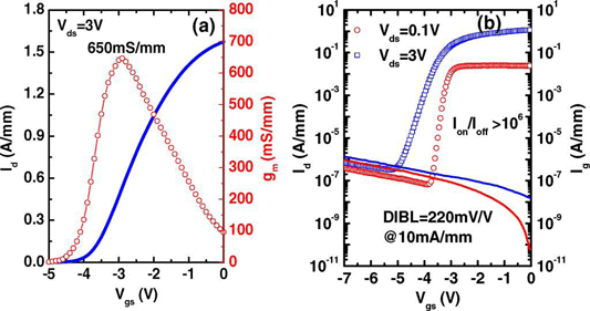
Figure 2: Transfer characteristics of InAlN/AlN/GaN HEMT at 3V and 0.1V drain biases: (a) linear scale and (b) semilog scale.
On the plus side, the on–off ratio is more than six orders of magnitude (i.e. a factor of a million). The researchers also attribute the good pinch-off to “low gate leakage resulting from the blanket DFP treatment”. The three-terminal breakdown for 1mA/mm at –12V gate potential was 30V.
The frequency performance was measured between 250MHz and 110GHz, giving a current gain cut-off (fT) of 370GHz after correcting for the effects of parasitics (de-embedding). The uncorrected fT was 160GHz. The researchers comment: “To the best of our knowledge, an fT of 370 is the highest reported in any GaN-based HEMT”.
Unfortunately, the maximum oscillation (fMAX) was low, at 30GHz (27GHz pre-de-embedded) “due to the high gate resistance induced by the rectangular gate”.
Based on analysis of various delay effects, the researchers believe that 500GHz fT should be possible with shorter gates. To improve the fMAX value, more work is needed on reducing parasitic effects and improving the transconductance through better electrostatic control of the channel. One way to do the latter may be to use AlN/GaN/AlN quantum well structures.
The work was supported by grants from the US Defense Advanced Research Projects Agency (DARPA) and the US Air Force Office of Scientific Research.