- News
29 June 2012
Hybrid ohmic-Schottky drain for higher breakdown in nitride HEMTs on silicon
Taiwan National Tsing Hua University has used a hybrid ohmic-Schottky drain to reduce buffer leakage and improve breakdown performance in aluminium gallium nitride (AlGaN) semiconductor transistors produced on silicon substrates [Yi-Wei Lian et al, IEEE Electron Device Letters, published online 11 June 2012]. By combining ohmic and Schottky drain regions, the Tsing Hua researchers increased breakdown voltage by up to 65% with almost no degradation of on-resistance.
In the target application of high-power switching, buffer leakage causes significant power loss. Apart from the quality of the buffer growth process, the ohmic source-drain alloying process can also affect buffer leakage by introducing metal spikes into the nitride semiconductor. Such spikes focus electric field lines, inducing leakage currents and breakdown.
Recently, Schottky drain contacts have been proposed as a way to reduce buffer leakage. However, Schottky contacts have a non-linear current-voltage behavior, adding a turn-on voltage that increases on-resistance.
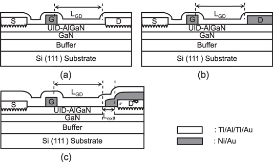
Figure 1: Cross sections of AlGaN/GaN HEMTs on silicon with different types of drain electrodes: (a) ohmic drain, (b) Schottky drain, and (c) hybrid drain.
The Tsing Hua researchers tested the different drain electrode structures (Figure 1) using two epitaxial material samples. Sample A consisted of a 1μm GaN buffer/channel, followed by a 24nm Al0.25Ga0.75N barrier. Sample B was more complex, with a 3.3μm GaN buffer, 1.5μm GaN channel, 20nm Al0.25Ga0.75N barrier, and a 1nm GaN cap.
Although the researchers did not have exact knowledge of the growth process for the samples, they point out that buffer layers usually begin with AlN to prevent diffusion of Ga into the silicon substrate. Further AlN or AlGaN layers are often incorporated into the buffer to relax strain from the large lattice mismatch and block threading dislocations to improve material quality in the channel layer.
Hall-effect and electrical measurements on the samples indicate similar performance, with the mobility and carrier density of sample A being 1519cm2/V-s and 8.6x10¹²/cm2, respectively. The corresponding figures for B were 1492cm2/V-s and 9.7x10¹²/cm2. The sheet resistances for A and B were, respectively, 476Ω/square and 432Ω/square.
Device processing began with isolation using a 300nm chlorine/argon inductively couple plasma (ICP) etch. The ohmic areas were patterned using photolithography and then treated with argon ICP to reduce contact resistance. The ohmic contact metals were titanium/aluminium/titanium/gold, applied using electron-beam evaporation and annealed at 800°degreeC in nitrogen for 30 seconds. The Schottky for the gate and drain (where appropriate) contact metals consisted of nickel/gold. The process was completed with multi-layer surface passivation with silicon nitride and silicon oxide applied with plasma-enhanced chemical vapor deposition (PECVD).
The different device types (Figure 1) were produced near to each other on the samples to ensure fair comparison. The hybrid device has a Schottky extension of 3μm towards the gate. However, the gate-drain separation is kept the same as the comparison devices to allow fair assessment of the breakdown voltage. The Schottky extension provided a field-plate shaped like the capital Greek letter ‘gamma’ (i.e. Γ). This avoids electric field concentrations that occur with the ohmic drain. Breakdown occurs at high electric field.
The drain contact is a square region with the gate and source electrodes as concentric square rings around the drain. The square layout is designed to “reduce the gate leakage current and mitigate the effects of traps originating from the dry etching damage at the sidewall of the mesa edge”.
The devices had a fixed gate-source distance of 2μm and a gate width of 400μm (the length of the square line). The gate-drain distance was varied between 5μm and 20μm. The threshold voltage was negative, at -2.9V, giving normally-on ‘depletion-mode’ operation (i.e. current flows at zero gate potential).
Devices with ohmic, Shottky and mixed drain contacts showed similar saturation current levels at +1V gate potential. The pure Schottky contact required a turn-on voltage of about 1V, increasing on-resistance. By contrast, devices with mixed ohmic-Schottky drain showed no onset voltage. In figures, the on-resistances were 1.78mΩ-cm2, 2.33mΩ-cm2, and 1.80mΩ-cm2 for ohmic, Schottky, and hybrid drains, respectively.
The hybrid devices also demonstrated the largest breakdown voltages (Figure 2) in three-terminal breakdown measurements (1mA/mm drain current in -10V gate, off-state). The researchers believe the improved performance of the hybrid drain is due to there being two electric field peaks – at the edges of the Schottky and ohmic regions – rather than one, as in the cases of the single-electrode-type devices. “This twin peak distribution can effectively alleviate and smooth out the electric field intensity around the drain side,” the researchers comment.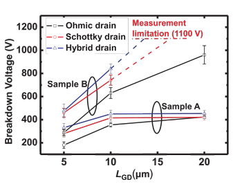
Sample A devices with thinner buffer layer had lower breakdown voltages. The breakdown voltage also apparently saturates at 400-450V for large gate-drain distance, due it is thought to leakage through the buffer.
Figure 2: Breakdown voltage as a function of the gate-drain spacing with three different structures at -10V gate.
For sample B devices, the increase in breakdown voltage for a 5μm gate-drain distance over ohmic drains was 60% (170V) and 65% (187V) for Schottky and hybrid drains, respectively. At 10μm gate-drain, the increases were 18% (112V) and 33% (210V), respectively.
Sample B devices with a 20μm gate-drain distance also had order-of-magnitude reductions in off-state (-10V gate) leakage current. “This can be attributed to the Schottky drain metal with a smooth contact interface, which can reduce the high electric field around the metal spikes and suppress the buffer leakage current,” the researchers write.
The author Mike Cooke is a freelance technology journalist who has worked in the semiconductor and advanced technology sectors since 1997.