- News
12 June 2012
Copper wiring for nitride semiconductor HEMTs
Taiwan-based researchers have been working to reduce nitride semiconductor high-electron-mobility transistor (HEMT) costs by developing copper interconnect structures compatible with production processes on silicon substrates [Yueh-Chin Lin et al, Appl. Phys. Express, vol5, p066503, 2012]. The collaborators are at National Chiao-Tung University and National Chung-Cheng University.
Nitride HEMTs are being developed for power device applications due to the high breakdown voltages, high electron saturation velocities and high temperature operation that are possible. In conventional production processes, gold wiring is used as the major interconnection metal.
Unfortunately, gold is expensive, with gold prices fluctuating between $1500-1900/ounce in the past year; raw copper has varied between $3 and $4.50 per pound (19-28 cents/ounce). However, it is presumably more expensive to create the pure copper needed for semiconductor processing, and the densities are somewhat different, leading the Taiwan researchers to estimate that copper is 400 times cheaper than gold.
Further attractive properties of copper include lower resistivity (1.67μΩ-cm versus 2.2μΩ-cm) and higher thermal conductivity (4.01W/cm-K versus 3.18W/cm/K).
The drawback with copper is that it is not compatible with high-performance nitride semiconductor devices. A vital requirement, therefore, is finding a good barrier against diffusion of copper into the underlying nitride semiconductor device.
The epitaxial layers for the Taiwan devices were grown on silicon using metal-organic chemical vapor deposition (MOCVD) and consisted of AlN, AlGaN buffer, GaN channel, AlN spacer, AlGaN Schottky barrier, and GaN cap. The ohmic source-drain contacts consisted of titanium/aluminum/nickel/gold annealed at 800°C for 60 seconds in nitrogen. Mesa isolation structuring was performed with a chlorine inductively coupled plasma etch.
 The gate region was defined using photolithography. The Schottky gate contact consisted of nickel/gold. Device passivation was provided by a silicon nitride film. Access to the contacts was achieved by etching through the passivation.
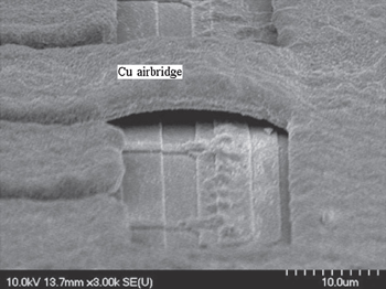
Figure 1: SEM image of the GaN HEMT with Cu airbridges by using Ti/Pt/Ti/Cu multilayer diffusion barrier.
Seeds for the interconnects were sputtered with diffusion barrier layers of titanium/platinum/titanium followed by copper. Further copper was applied through electrolysis using a copper sulfate
(CuSO4·5H2O) electrolyte. The interconnect structures included air-bridges (Figure 1).
Auger electron spectroscopy (AES) showed that the diffusion barrier was effective with an anneal at 350°C for 30 minutes, but that a 400°C for the same amount of time produced diffusion of the gold and copper towards each other, which would result in device deterioration.
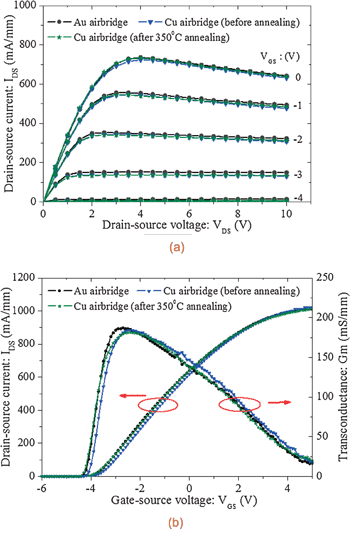 Devices with 50μm x 4μm gates produced using copper interconnects, including air-bridges, showed comparable performance to HEMTs with gold-based structures (Figure 2). The maximum drain-source current for a non-annealed HEMT was 1020mA/mm, compared with 1010mA/mm for devices with gold-based interconnects. The threshold voltages were -4.1V and -4.2V for the copper and gold interconnected HEMTs, respectively. The respective peak extrinsic (uncorrected) transconductances at 10V drain bias were 184mS/mm and 187mS/mm.
Figure 2: DC characteristics of the 50μm x 4μm-gate Cu-metallized GaN HEMT before and after annealing at 350°C for 30 minutes: (a) drain current versus voltage curves, and (b) extrinsic transconductance and IDS versus gate potential curves.
After 350°C annealing for 30 minutes, the maximum drain current was 1012mA/mm, the threshold voltage was -4.3V, and the peak extrinsic transconductance was 181mS/mm. Stress at a drain bias of 28V showed only a small increase in current up to 24 hours stress time. The researchers comment that these results indicated that the material system was “quite stable”.
The author Mike Cooke is a freelance technology journalist who has worked in the semiconductor and advanced technology sectors since 1997.