- News
27 July 2012
Smallest semiconductor laser emits CW green light below 3D diffraction limit
Physicists at The University of Texas at Austin, in collaboration with colleagues at Taiwan’s National Tsing-Hua University and National Chiao-Tung University and at the Beijing National Laboratory for Condensed Matter Physics and Institute of Physics, Chinese Academy of Sciences, have developed what is claimed to be the world’s smallest semiconductor laser, with photonic applications ranging from computing to medicine (Y.-J. Lu et al, ‘Plasmonic Nanolaser Using Epitaxially Grown Silver Film’, July 27 issue of Science).
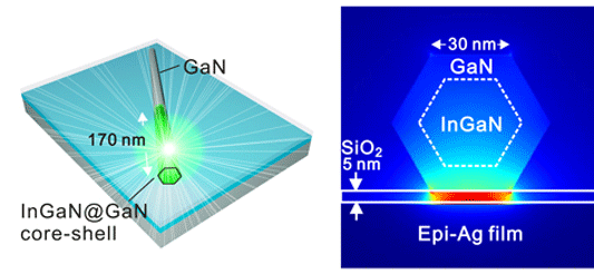
Graphic: Nanoscale structure used for demonstrating ultralow-threshold nanolaser. A single nanorod is placed on a 28nm-thick silver film. The resonant electromagnetic field is concentrated at the 5nm-thick silicon dioxide gap layer sandwiched by the nanorod and the atomically smooth silver film.
The researchers say that miniaturizing semiconductor lasers are key to the development of faster, smaller and lower-energy photon-based technologies, such as ultrafast computer chips; highly sensitive biosensors for detecting, treating and studying disease; and next-generation communication technologies. Such photonic devices could use nanolasers to generate optical signals and transmit information, and have the potential to replace electronic circuits. However, the size and performance of photonic devices have been restricted by the three-dimensional optical diffraction limit (limiting the ability to distinguish between two objects separated by a distance of less than about half the wavelength of the light).
“We have developed a nanolaser device that operates well below the 3D diffraction limit,” says Chih-Kang ‘Ken’ Shih, professor of physics at The University of Texas at Austin. “We believe our research could have a large impact on nanoscale technologies,” he adds.
Shih and his colleagues have reported the first continuous-wave (CW) operation of a low-threshold laser below the 3D diffraction limit. When operated, the nanolaser emits green light. The laser is also too small to be visible to the naked eye.
The device is constructed from a gallium nitride (GaN) nanorod that is partially filled with indium gallium nitride (InGaN), both commonly used materials in LEDs. The single InGaN/GaN core-shell nanorod gain medium is placed on top of a thin (5nm-thick) insulating layer of silicon dioxide that in turn covers a 28nm-thick atomically smooth layer of silver film deposited by molecular beam epitaxy (MBE).
Shih’s lab has been developing the material for more than 15 years. The atomic smoothness is key to building photonic devices that do not scatter and lose plasmons (waves of electrons that can be used to move large amounts of data). “Atomically smooth plasmonic structures are highly desirable building blocks for applications with low loss of data,” says Shih.
Nanolasers such as this – i.e. a SPASER (surface plasmon amplification by stimulated emission of radiation) - could provide for the development of chips where all processes are contained on the chip, which could prevent heat gains and information loss typically associated with electronic devices that pass data between multiple chips, the researchers say.
“Size mismatches between electronics and photonics have been a huge barrier to realize on-chip optical communications and computing systems,” says Shangjr Gwo, professor at Taiwan’s National Tsing Hua University and a former doctoral student of Shih’s.
Shih and Gwo’s colleagues include Gennady Shvets, professor of physics at The University of Texas at Austin, and Lih-Juann Chen, professor at National Tsing Hua University.