- News
5 July 2012
Boron nitride release transfer of nitride LEDs from sapphire to adhesive tape
NTT Basic Research Laboratories in Japan has used hexagonal boron nitride (h-BN) layers to release nitride semiconductor light-emitting diodes (LEDs) from sapphire and transfer them to commercially available adhesive tape [Toshiki Makimoto et al, Appl. Phys. Express, vol5, p072102, 2012].
Commercial production of nitride LEDS tends to be performed on sapphire substrates, since the alternatives such as silicon carbide (SiC) and free-standing gallium nitride (GaN) are much more expensive. Some research has been directed to producing nitride LEDs on silicon (e.g. Nitride LED transfer from silicon to copper increases light output by 122%), but the substrate in that case strongly absorbs the emitted light.
Although LEDs on sapphire do not suffer the latter problem, they do experience strong self-heating effects that degrade performance. The self-heating occurs due to the low thermal conductivity of sapphire. Therefore, methods using laser lift-off or etch have been developed to remove the substrate. However, these methods can be time consuming (expensive) and/or can damage the performance of the LED.
Recently, NTT has reported the use of h-BN interlayers to allow simple mechanical release of devices from sapphire in seconds (Mechanical release of nitride semis from sapphire using boron nitride layer). The h-BN is structured like multi-layer graphene/graphite with strong in-plane bonds and weak inter-plane bonds, allowing such release. The researchers have now named their process ‘Mechanical Transfer using a Release layer’ (MeTRe).
The researchers see potential applications of MeTRe as including transfer to flexible substrates, the integration of blue and green nitride LEDs with red phosphide-based LEDs, the combination of nitride with other photovoltaic solar cells produced in other material systems, and the integration of GaN-based devices with silicon complementary metal oxide semiconductor (CMOS).
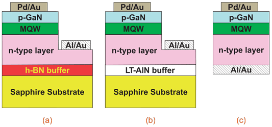
The 3nm h-BN buffer was deposited on sapphire using metal-organic vapor phase epitaxy (MOVPE) of triethyl-boron and ammonia. Further layers consisted of a 300nm aluminium gallium nitride (AlGaN) buffer (16%-Al), a 3μm silicon-doped n-GaN, 10x InGaN/GaN multi-quantum well (15%-indium, 1.8nm/8.6nm), and 100nm of magnesium-doped p-GaN. A conventional structure with a low-temperature (LT) AlN buffer in place of the BN was also created for comparison.
Two LEDs were created in a fairly standard format with the p- and n-electrodes on the same side of the device, giving regions of lateral current flow (Figure 1a, b). A third device was also produced with vertical electrodes (Figure 1c). The vertical format is only possible with release from the electrically insulating sapphire growth substrate.
When tested at 20mA injection current, the conventional device emitted at a wavelength around 450nm and the BN devices around 460nm. The slight difference in violet-blue wavelength was probably due to different MOVPE growth conditions, according to the researchers. The lateral LED on BN had about three times the peak height of the conventional LED, although the researchers merely state that the performance is “comparable to or stronger than that of the lateral LED”.
The vertical LED had a slightly reduced peak height compared with the lateral LED on BN, but it was still stronger than the conventional LED. In fact, the vertical LED spectrum consisted of a series of overlapping peaks around 14nm apart. These peaks were attributed to interference between directly emitted light and light reflected from the aluminium/gold n-electrode. The 14nm peak separation is consistent with the thickness and refractive index of the nitride semiconductor material making up the LED.
The researchers comment: “The observation of the multiple peaks in the EL spectra means that the underside surface is very smooth after being released from the sapphire growth substrate.”
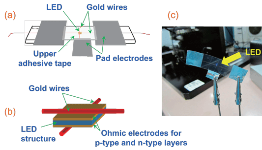
The researchers also assembled the vertical LED into a structure consisting of a chip between crossed gold wires, and then this structure was sandwiched between two pieces of 46μm-thick commercial adhesive tape (Figure 2). The completed structure was less than 0.1mm thick.
The researchers conclude: “Our newly developed MeTRe method will open the way to releasing and transferring a wide range of GaN-based devices to large-area, flexible, and affordable substrates.”
Nitride LED transfer from silicon to copper increases light output by 122%
Mechanical release of nitride semis from sapphire using boron nitride layer
Boron nitride GaN LEDs Sapphire
The author Mike Cooke is a freelance technology journalist who has worked in the semiconductor and advanced technology sectors since 1997.