- News
23 July 2012
Graphene-SiC transistor shows way to new integrated circuits
Friedrich-Alexander University Erlangen-Nuremberg, Germany, and ACREO AB, Sweden, have developed a transistor technology combining graphene with silicon carbide (SiC) [S. Hertel et al, Nature Communications, published 17 July 2012].
Graphene is a remarkable material that scientists are keen to exploit, with properties such as extremely high mobility (~106cm2/V-s), high current stability (6mA/μm), and high temperature stability and thermal conductivity. While it has been fairly easy to induce metallic behavior in graphene, active switching/semiconductor properties have been more elusive.
The German/Swedish collaboration has rather used the semiconductor properties of the SiC substrate that they use to create graphene. The ohmic source-drain and Schottky contacts are formed from creating different interface properties between the SiC substrate and the graphene surface.
The process requires only a lithography step, allowing the creation of transistors, diodes, and resistors. Ultimately, the researchers hope to create a method for integrated circuits that contain only graphene interconnects.
“The material combination graphene on SiC thus combines two of the most robust materials for electronic applications we are aware of, and both materials are in intimate, epitaxially defined contact,” the researchers comment.
The transistors were created on 6H polytope SiC substrates (3.5° off (0001) direction) with epitaxial 3μm p-SiC and 2.9μm n-SiC layers applied using chemical vapor deposition (CVD). The pn junction creates vertical confinement of the channel to the lightly n-doped top layer.
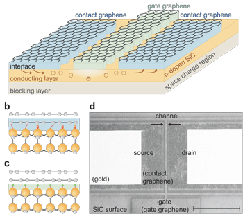 The ohmic contact monolayer graphene (MLG) was created using thermal decomposition of the SiC at 1650°C in argon flux near room pressure. Device mesas were formed using reactive ion etch.
Figure 1: Two different epitaxial graphene materials combined in a monolithic transistor: schematic (a); side views of ohmic contact graphene for source and drain (b), and Schottky-like gate graphene (c); electron micrograph showing the device geometry (d).
The gate structure is formed by converting the MLG to quasi-free-standing bilayer graphene (QFBLG) by thermal annealing at 540°C, 880mbar for 90 minutes in hydrogen. Holes of 200nm diameter at 0.5μm separation are created in the MLG beforehand to allow hydrogen into the regions where conversion is desired. The device structures were then patterned and etched.
Finally, the metal source-drain contacts of titanium/gold and Schottky gate contacts of nickel were applied. Also, a nickel contact was made to the p-SiC substrate layer to allow a back-gate control of the space-charge/channel thicknesses resulting from the pn junction. This is particularly useful for a prototype device, but would not be required in manufactured components when performance has been optimized in development.
Contact of MLG with n-SiC gives an electron density of 1013/cm2 and mobility of 900cm2/V-s. The QFBLG has a hole density of 1013/cm2 and mobility of 2000cm2/V-s, giving a Schottky contact with the underlying n-SiC.
While the MLG contact gives ‘perfectly ohmic behavior’, unlike metal contacts on SiC, the QFBLG Schottky gate performance suffers from a spread of barrier heights and sample-to-sample fluctuations, indicating strong dependence on surface quality and therefore scope for improvements through better process control. Further, the contact resistance of the MLG can be improved from 63mΩ-cm2 to 6μΩ-cm2, through 1019/cm3 nitrogen doping of the underlying lightly doped SiC (carrier density 1015/cm3, mobility 370cm2/V-s).
The transistor could be put into normally-on or normally-off modes, depending on the back-gate potential (Figure 2). Normally-on behavior was achieved for a back-gate bias of -2.5V. At room temperature (294K), the on-off ratio was 2100 with a minimum drain current of 0.36nA at a drain bias of 0.1V. A back-gate bias of -4V gave normally-off behavior with the space-charge regions of the unbiased graphene top-gate and of the pn junction back-gate meeting. Positive top-gate bias opened the channel, giving up to 12,000x on-current. The disadvantage was the forward-bias in the Schottky gate, leading to gate leakage. Improved on/off performance in both modes could be achieved with temperature reduction to 220K.
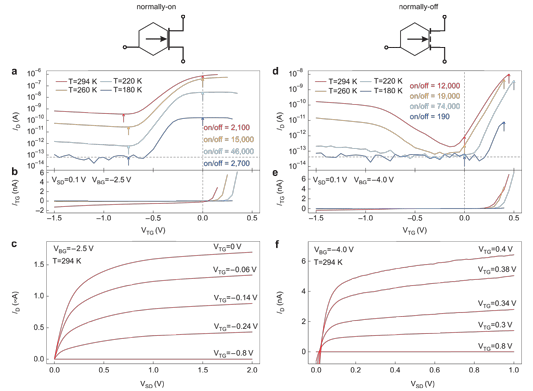
Figure 2: Electrical characterization of a monolithic epitaxial graphene transistor. Transfer characteristics (a) and gate leakage currents (b) for various temperatures, and output characteristics (c) at room temperature in the normally-on operation mode. On/off ratios were determined between the current at 0V top-gate voltage and the minimum drain current value (indicated by arrows). (d–f) Corresponding plots for normally-off operation mode.
The large scale of the device and the conductive substrate meant a modest frequency performance that showed no significant damping/phase shift and no signal distortion up to 1MHz, in line with theoretical expectations. A vanadium implant to give semi-insulating SiC in the transistor periphery could boost the frequency cut-off by up to 30x. “The route for further speed improvements is obvious: optimization and shrinkage of the geometry, reduction of source, drain resistances, and so on,” the researchers add.
Graphensic spun off from Sweden’s Linköping University for graphene-on-SiC epi
Graphene-SiC transistor SiC Graphene
The author Mike Cooke is a freelance technology journalist who has worked in the semiconductor and advanced technology sectors since 1997.