- News
17 January 2012
All-silicon light emission through nanocrystal confinement
Researchers in Australia and Italy have demonstrated all-silicon light-emitting diodes (LEDs) using p-type silicon nanocrystals produced by material technology that has been developed for third-generation photovoltaics (PV) [Dawei Di et al, Appl. Phys. Lett., vol99, p251113, 2011]. The electroluminescence from the devices ranged from the visible to infrared, with emissions strongest at 750nm, 980nm and 1150nm, depending on the barrier material (silicon dioxide or silicon nitride). The research team consisted of participants from University of New South Wales, University of Sydney, and University of Trento.
In bulk silicon (c-Si), the emission and absorption of light are severely constrained by the need to conserve crystal momentum of the electrons and holes. Emission is particularly difficult since the thermally excited holes and electrons have very different crystal momentums — that of the holes is around zero since the valence band has its peak there, but electrons gather in six valleys at the conduction band edge, away from zero. The normal LED process of electron–hole recombination producing a near-zero-momentum photon is thus very unlikely.
With Si nanocrystals (NCs), it is hoped to use quasi-particle confinement of the electrons and holes to introduce momentum uncertainty (Heisenberg’s Δx x Δp ≥ ħ/2) to improve probabilities for both absorption (PV) and emission (LED).
The device material (Figure 1) was constructed by radio-frequency sputtering of 30 bi-layers consisting of 2nm of silicon nitride (or silicon dioxide) and 4nm of boron-doped silicon-rich oxide (SRO) onto n-type silicon wafers. The boron doping gives p-type conduction in silicon. After the deposition, the material was annealed at 1100°C in nitrogen for 1 hour to create the silicon nanocrystals.
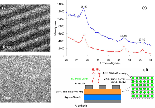
Figure 1: Structural information of materials and devices. HRTEM images of the samples with (a) Si3N4 barriers and (b) SiO2 barriers. The dark stripes are Si3N4 barriers. The light grey areas correspond to SiO2 and the dark grey ‘clouds’ are Si NCs. (c) XRD patterns of the samples with Si3N4 barriers (upper curve) and SiO2 barriers (lower curve). (d) Schematic diagram of a Si NC/c-Si diode.
X-ray and electron microscope measurements gave typical sizes for the silicon nanocrystals of 3–5nm. Crystals in silicon dioxide (SiO2) seem to be of better quality than those in silicon nitride (Si3N4), according to x-ray analysis.
Aluminum front and rear electrodes were deposited with windows cut on the nanocrystal side using photolithography techniques. A rather high series resistance was found in current–voltage measurements: 240Ω for the silicon dioxide structure and 100Ω for the silicon nitride. The high values are blamed on the multiple numbers of tunneling dielectrics and interfaces, along, possibly, with use of non-ideal metal contacts and current crowding due to unoptimized material structure and metallization.
Clear electroluminescence signals were seen with voltages exceeding 5V (Figure 2). The emissions fell in the 500–1200nm wavelength range, as detected by nitrogen-cooled silicon and indium gallium arsenide (InGaAs) charge-coupled detectors (CCDs). The short-wavelength end is blue-green and the long-wavelength end is infrared. The red/infrared border comes at ~740nm.
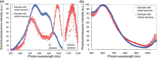
Figure 2: Normalized (a) electroluminescence and (b) photoluminescence spectra of Si NC/c-Si diodes with different barrier dielectrics (at room temperature ~ 300K).
With the silicon dioxide barriers, the researchers see three main humps at 720nm, 980nm and 1150nm, with a weaker structure at ~870nm. The team ascribes the 1150nm peak to the crystalline bulk silicon. However, the 980nm peak is 0.145eV higher than the silicon bandgap of 1.12eV. The researchers associate the 720nm peak with nanocrystal transitions with a gap of almost 1.7eV.
The silicon nitride devices have a stronger peak at 750nm that is also associated with nanocrystals. The shift in wavelength is ascribed to the lower quantum confinement offered by silicon nitride (gap ~5.3eV) barriers, compared with silicon dioxide (~9eV). Also, with a lower barrier, carriers can tunnel into the nanocrystals more easily. A secondary peak in the silicon nitride device is seen at 870nm and the 980nm peak is very weak. No emissions were seen in the 1050–1200nm range of the InGaAs detector. It is thought that the higher tunneling probability could lead to a larger nanocrystal emission signal compared with other channels, enhancing the 750nm peak at the expense of the others.
Photoluminescence excited by a 409nm laser was also measured. The nanocrystal peak blue-shifted to the shorter wavelength of 600nm (2.06eV). The researchers say that they are still discussing the source of the shift.
The team says that the devices are far from optically and electrically optimized and that “their strengths and limitations are yet to be tested in further studies”. One of the first steps will be to study color tunability achieved through tailoring the nanocrystal sizes.
Squeezing light out of silicon
p-type silicon nanocrystals Silicon dioxide Silicon nitride
http://link.aip.org/link/doi/10.1063/1.3671671
The author Mike Cooke is a freelance technology journalist who has worked in the semiconductor and advanced technology sectors since 1997.