- News
3 January 2012
Zinc oxide transparent conduction on semipolar nitride LEDs boosts EQE
Researchers in the USA and Korea have been developing zinc oxide (ZnO) as a transparent conducting material for use with light emitting diodes (LEDs) constructed from (10-1-1) semipolar nitride semiconductor material [Jacob J. Richardson et al, Appl. Phys. Express, vol4, p126502, 2011].
The use of semipolar or even nonpolar III-nitrides is designed to overcome polarization field effects that arise spontaneously and in strained piezoelectric conditions such as the quantum confined Stark effect (QCSE). These fields are strongest along the standard c-direction of the nitride semiconductor lattice. The University of California Santa Barbara has been researching semipolar and nonpolar devices for some time. The Korean researcher, Jun-Seok Ha, came from Chonnam National University, Republic of Korea.
In nitride LED devices, performance can be improved by avoiding current bunching effects due to the less than ideal conductivity of the p-type layers. Transparent conducting layers can help spread the current, while allowing light to emerge from the device. Indium tin oxide (ITO) is frequently used for such purposes in LEDs and in solar cells. However, indium is a rare material and the use of a less costly material such as zinc would be preferred in manufacturing.
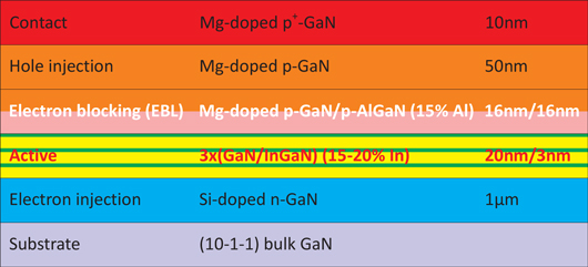
Figure 1: Epitaxial structure used for LEDs.
The USCB/Chonnam team grew their devices on (10-1-1) bulk gallium nitride (GaN) substrates supplied by Mitsubishi Chemical. Atmospheric-pressure metal-organic chemical vapor deposition (MOCVD) was used to grow multiple films of various alloys involving indium, aluminum and gallium nitrides (InAlGaN, Figure 1).
 The ZnO transparent layer was grown using a low-temperature aqueous solution (pH 12 ammonia with dissolved ZnO). The substrates were suspended in the aqueous solution for 18 hours at 90°C.
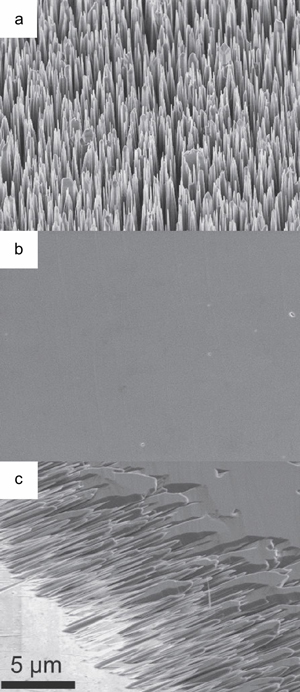
Unlike previous work with c-plane GaN, the researchers found that they did not need separate nucleation or “seeding” steps or solution additives to modify the morphology. For the c-plane growth these extra steps/additives avoid the formation of needle structures, rather than the desired
smooth coalesced film (Figure 2). Further study of the sample holder region (Figure 2c) suggested that the growth even on the (10-1-1) GaN starts as needles pointing in the c-direction, but that these needles then coalesced to form a smooth film.
Figure 2: Representative SEM images showing the ZnO morphology resulting from identical growth conditions on (a) (0001) and (b) (10-1-1) GaN substrates. An uncoalesced region of the same (10-1-1) film from (b) is shown in (c).
X-ray studies suggested that the planes of the ZnO were tilted 0.4° in the c+ direction. Such tilting has been found to be a misfit strain release mechanism in semipolar GaInN and GaAlN films, but the researchers say that they need further work to understand the nature of the ZnO tilt.
Thicker layers of ZnO were applied in multiple steps. The first layer was annealed at 500°C in oxygen-nitrogen (20% O2) gas for 15 minutes to improve adhesion of subsequent layers. Without this annealing step, the entire film of thicker layer ZnO would occasionally delaminate.
LEDs were then created using standard processes such as chlorine plasma etch to the n-type layer, forming 2x0.5mm mesas, and electron beam deposition of the contact metals. The backside of the wafer was roughened to reduce light reflection at the sapphire-air interface that reduces the light extraction. The singulated chips were packaged in a vertical stand transparent LED architecture.
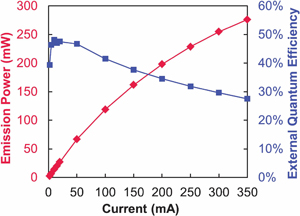 Figure 3: Light emission power and external quantum efficiency of a semipolar (10-1-1) LED using an epitaxial ZnO current-spreading layer deposited from low-temperature aqueous solution. Measurements were performed under pulsed current conditions (1% duty cycle).
Pulsed measurements (1% duty cycle, Figure 3) gave 27mW light output power at current density 2A/cm2, and 276mW at 35A/cm2. The maximum external quantum efficiency (EQE) reached 48% at 1A/cm2. At the highest current density of 35A/cm2, this had fallen to 27.5%.
The researchers comment: “The light output and EQE of the device using the ZnO were lower than results previously published for a similarly packaged (10-1-1) device using an ITO current-spreading layer.”
The team points out that due to the smallness of the substrate available, they were unable to compare their ZnO-covered device with one using ITO. The difference in performance with the earlier experiment could be down to difference in quality of the substrates or in run-to-run process variations in the MOCVD growth of the epitaxial material, they say.
“These results indicate that aqueous solution deposited epitaxial ZnO films appear promising as current-spreading layers for semipolar GaN LEDs, but more work will be necessary to analyze and optimize performance, as well as understand the nature of the epitaxial interface,” the researchers conclude.
ZnO transparent conduction Semipolar nitride LEDs GaN
The author Mike Cooke is a freelance technology journalist who has worked in the semiconductor and advanced technology sectors since 1997.