- News
30 January 2012
Increased mobility and reduced residual electron concentration indium nitride
Researchers based in China and Germany have used boundary-controlled temperature molecular beam epitaxy (MBE) to improve indium nitride (InN) quality, giving the best mobility and residual electron concentration figures achieved so far [Xinqiang Wang, Appl. Phys. Express, vol5, p015502, 2012]. The work was carried out by researchers at Peking University, Hong Kong University of Science and Technology, Helmholtz-Zentrum Dresden-Rossendorf (HZDR),
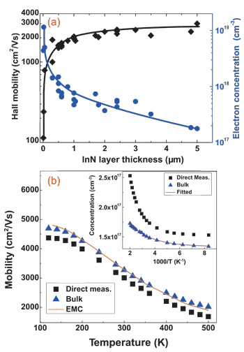 Direct measurements of Hall characteristics of the InN material varied with layer thickness (Figure 1a), giving an increase in mobility and decrease in electron concentration. At 5μm, the Hall mobility reaches 3010cm2/V-s and the residual electron concentration is 1.77x10¹⁷/cm3. These values compare with previous reports of 2370cm2/V-s electron mobility and down to 3x10¹⁷/cm3 residual electron concentration.
Figure 1: (a) Directly measured Hall mobility (diamonds) and residual electron concentration (circles) of InN layers as functions of layer thickness. Lines are merely guides for the eye. (b) Temperature-dependent mobilities and (inset) electron concentrations: solid squares are directly measured values and solid triangles are extracted values for InN bulk layer. Solid line is ensemble Monte Carlo (EMC) result. Electron concentration in bulk layer is fitted by standard single shallow-donor.
Temperature-dependent measurements were also carried out on the 5μm InN layer between 120K and 500K. At the lowest temperature, the mobility reached 4370cm2/V-s.
InN has a narrow bandgap of 0.63eV and low effective mass for the electron of about 0.055 that of the free-space value. Low effective masses tend to be associated with high mobility. However, growing high-quality InN is a challenge.
Defects, impurities, non-uniformities etc reduce mobility through electron scattering effects and tend to increase the number of electrons in the conduction band. Achieving p-type conductivity through holes in the valence band is difficult to achieve in nitride semiconductors anyway, and large numbers of residual electrons just makes it harder.
One of the major spurs to InN study is the prospect of the wide electromagnetic wavelength range potentially accessible to alloys of the InN (~1970nm, infrared), gallium nitride (3.4eV~365nm, ultraviolet), aluminum nitride (6.2eV~200nm, deep UV) semiconductor material system. The higher mobility of up to 3010cm2/V-s is also attractive for high-speed electronics. Bulk mobility in gallium nitride is usually less than 1000cm2/V-s. Higher values can be attained in confined ‘two-dimensional electron gas’ (2DEG) structures at nitride semiconductor interfaces.
InN grows at best quality in MBE when the temperature is maintained close to the maximum before dissociation at around 500°C. MBE growth temperatures for the other nitride semiconductors are higher (typically at least 700°C for gallium nitride, more than 800°C for aluminum nitride). Temperature control using a thermocouple is tricky since, as the material grows, the location of the temperature reading recedes from the growth front. Hence one has to reduce the temperature of the thermocouple reading control point to maintain 500°C at the growth point.
The Peking/Hong Kong/HZDR InN layers were grown with a GaN buffer on sapphire by MBE using an SVT Associates system. Buffer layers grown both by MBE and metal-organic chemical vapor deposition (MOCVD) were used. Indium-rich conditions were used for InN growth.
In addition to the direct measurements quoted earlier, the researchers also sought to correct the characteristics for the electron-accumulation effect that has been found for InN layers. This effect results in electrons collecting on the surface of the material, affecting measurements of mobility and conductivity.
Peking University has recently measured the properties of the surface electron-accumulation layer, and these results were used to extract bulk values (Figure 1b). The room-temperature value for bulk mobility was increased to 3280cm2/V-s and residual electron concentration reduced to 1.47x10¹⁷/cm3.
The temperature-dependent bulk mobility results were also modeled using an ensemble Monte Carlo (EMC) that included scattering effects from polar optical phonons, deformation potential and piezoelectric-mode acoustic phonons, ionized impurities, neutral impurities and threading dislocations. The electron concentration was fitted using a standard single shallow-donor level. A deep donor would not fit the results.
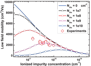 Further simulations suggest that with zero dislocations the mobility could reach ~10000cm2/V-s when the electron densities from ionized impurities were less than 1016/cm3 (Figure 2). In the more realistic situation of 1017-1018/cm3 densities, the mobility ranges between 6900cm2/V-s and 2600cm2/V-s. The adding of dislocation scattering mainly affects mobility at lower electron densities.
Figure 2: Calculated low-field electron mobility in InN as function of ionized impurity concentration at different dislocation density (Ndis) levels. Experimental results are bigger open diamonds.
The researchers comment: “From the theoretical result shown in Figure 2, we can see that it is very important to reduce the density of dislocations and electron concentration to improve the electron mobility.”
Comparison of the simulation with the experimental results for layers with thickness greater than 0.5μm shows comparability with the values for dislocation densities of 109/cm2. This dislocation level is slightly lower than that suggested by x-ray diffraction analysis, possibly due to only partial ionization of the dislocations.
Further x-ray analysis showed that the effect of growing thicker InN layers was to reduce the width of diffraction peaks, suggesting better crystal quality. The full-width at half-maximum (FWHM) of the peak from the symmetric (002) plane reduced from 900arcsec at 0.5μm thickness to 250arcsec at 5μm. The asymmetric (102) plane had a FWHM of 1600arcsec at 0.5μm and 820arcsec at 5μm.
“This implies that the densities of both the screw- and edge-component threading dislocations are reduced with increasing thickness, which is most likely the main reason for the reduction of electron concentration and improvement of electron mobility,” the researchers write.
The author Mike Cooke is a freelance technology journalist who has worked in the semiconductor and advanced technology sectors since 1997.