- News
6 January 2012
InGaAs gate all-arounder demonstrates shortest channel to date
Purdue and Harvard universities in the USA have presented the first demonstration of inversion-mode indium gallium arsenide (In0.53Ga0.47As) gate-all-around (GAA) metal-oxide-semiconductor field-effect transistors (MOSFETs) by a top-down approach [J. J. Gu, International Electron Devices Meeting, session 33.2, 2011].
Devices with III-V channels are attractive for increasing speed performance and decreasing power waste over mainstream logic devices using complementary MOS circuitry based on silicon channels. However, III-V devices suffer from short-channel effects such as poor values of off-state leakage, subthreshold slope, and drain-induced barrier lowering. These effects can be suppressed by using three-dimensional structures such as FinFETs and multi-gate formations. The ultimate structure in this trend is to have the channel surrounded by the gate electrode, giving the GAA device (Figure 1).
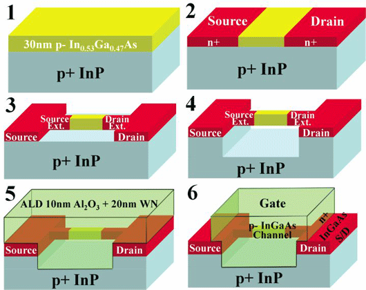
Figure 1: Schematic diagram of key process steps in the fabrication of InGaAs GAA MOSFETs.
The Purdue/Harvard comments on its achievement: “Benefiting from the GAA structure, we have demonstrated the shortest-channel-length (Lch = 50nm) III-V MOSFETs to date with well-behaved on- and off-state characteristics.”
Normalizing to the perimeter of the channel (i.e. 2x(height + width of fins) x number of channels), the typical on-current and extrinsic transconductance of a 50nm-long channel were 720μA/μm and 510μS/μm, respectively. A ‘hero’ device achieved an on-current of 1.17mA/micron (drain voltage 1V) and maximum transconductance of 701μS/μm.
The off-state is described as ‘reasonable’. The sub-threshold swing and drain-induced barrier lowering were 150mV/dec and 210mV/V, respectively. InGaAs quantum well devices have achieved (desirable) lower subthreshold swings of ~120mV/dec (Table 1).
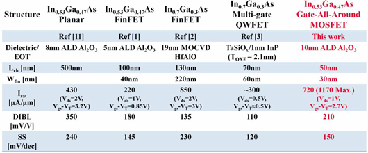
Table 1: Comparison of InGaAs GAA FETs in this work and recently reported top-down non-planar III-V FETs.
The 30nm p-type InGaAs channel was grown on heavily doped p-type indium phosphide (100) using molecular beam epitaxy (MBE). A 10nm layer of aluminum oxide was atomic-layer deposited for encapsulation. Source–drain regions of n-type material were formed with silicon ion implantation. Annealing at 600°C for 15 seconds in nitrogen was performed to activate the dopants.
The Al2O3 encapsulation was then removed with a buffered oxide etch. The channel was formed using photolithography and high-density plasma etch with boron trichloride and argon to make a fin structure. The channel was released by etching into the underlying InP with hydrochloric acid solution. The fins need to be patterned along the <001> direction for the HCl etch to select InP rather than InGaAs.
The surface of the released channel was passivated by soaking in ammonium sulfide. Then 10nm of Al2O3 gate insulator and 20nm tungsten nitride gate metal were grown in separate ALD processes. The gate etch was performed using carbon tetrafluoride and argon HDPE. The gate contact metals were chromium and gold. The source/drain contacts consisted of gold/germanium/nickel. Test pads consisted of titanium/gold.
Channel lengths from 50nm to 120nm and fin widths from 30nm to 50nm were tested with different numbers of parallel channels (1, 4, 9, 19).
The devices work in inversion mode, meaning that the channel is constructed of p-type material (majority carriers are holes), but the on-current is negatively charged ‘electrons’. However, unlike with traditional silicon complementary metal oxide semiconductor (CMOS) transistors, the threshold voltage is negative (–0.68V), giving a current when the gate potential is zero (i.e. normally-on). Normally-off, positive thresholds are preferred for low power consumption. The negative threshold is blamed on the low work function of the tungsten nitride gate metal.
Corrections for the effects of contacts gives an intrinsic transconductance of the channel of 750μS/μm. The relatively large effect of the contacts is blamed on non-optimal ion implantation, resistance from the channel/source–drain link, and the use of a non-self-aligned process.
The researchers believe that the subthreshold swing performance could be improved with thinner or higher dielectric constant gate insulation. Thinning the aluminum oxide to 5nm or 2.5nm should give substhreshold swings of 105mV/dec or 82mV/dec, respectively, on the basis of simple calculations.
The researchers comment: “Therefore a SS lower than 100mV/dec is achievable on surface-channel InGaAs MOSFETs at sub-100nm channel lengths with the current (NH4)2S surface passivation technique.”
The researchers expect that better performance could be obtained with InGaAs channels with indium content of 65–75%, “due to the higher electron mobility and the charge neutral level being closer to the conduction band edge”.
InGaAs buffer/channel structure boosts effective mobility 4.2x that of silicon
Increasing performance with III-V transistors on silicon
Self-aligned Ni-InGaAs as source–drain for InGaAs MOSFET
The author Mike Cooke is a freelance technology journalist who has worked in the semiconductor and advanced technology sectors since 1997.