- News
16 January 2012
NICT demonstrates first gallium oxide transistors
In collaboration with power conversion and magnetic product maker Tamura Co Ltd and optoelectronics engineering firm Koha Co Ltd, Japan’s National Institute of Information and Communications Technology (NICT) has developed and tested what it claims are the first single-crystal gallium oxide (Ga2O3) field-effect transistors (Higashiwaki et al, Applied Physics Letters vol. 100 (2012), 013504).
NICT says that Ga2O3 is a promising semiconductor material for high-breakdown and low-loss power devices because of its excellent material properties (such as a wide energy bandgap), which can reduce the cost and energy consumption of mass-produced devices.
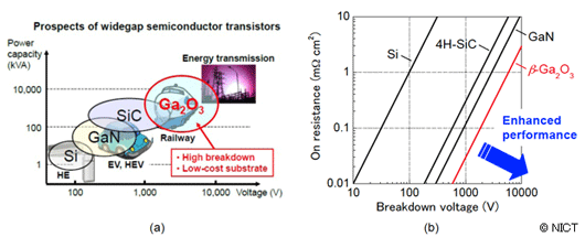
Figure 1: (a) Near-term applications of transistors. (b) On-resistance versus breakdown voltage of representative semiconductors and Ga2O3 for power devices.
Wide-bandgap semiconductors such as silicon carbide (SiC) and gallium nitride (GaN) can be used in high-breakdown and low-loss power devices. Figure 1(a) shows the prospects for Ga2O3 compared with these semiconductors, as estimated from their material properties. Figure 1(b) shows power device performance, which is determined by a trade-off between the two parameters breakdown voltage and on-resistance (hence the straight lines show the ideal performance limits of the materials). It can seen that Ga2O3 (toward the bottom-right corner of the graph) has better characteristics as a power device material than not only silicon but also SiC and GaN.
The researchers therefore expect that Ga2O3 power devices will initially have high-breakdown and high-power applications. Then, as Ga2O3 devices become more common, applications should broaden to those of SiC and GaN due to easy and low-cost substrate production.
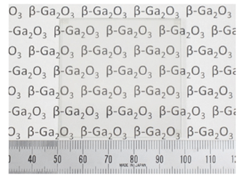 A feature of single-crystal Ga2O3 substrates is that they can be fabricated with the melt-grown method, unlike other wide-bandgap semiconductors such as SiC, GaN and diamond. Figure 2 shows a photograph of a 2-inch square single-crystal β-Ga2O3 substrate fabricated from melt. The melt-grown method is a low-energy-consumption, low-cost way to make large wafers because it does not need a high-temperature and/or high-pressure environment and its material efficiency is high. The method is especially suitable for mass production.
Figure 2: Two-inch square single-crystal β-Ga2O3 substrate fabricated by melt-grown method.
However, despite the material’s high potential, R&D on Ga2O3 electrical devices has lagged. The researchers therefore fabricated a Ga2O3 metal-semiconductor field-effect transistor (MESFET) by using newly developed technologies for making single-crystal substrates, epitaxial thin-film growth, and processing techniques to fabricate devices (a circular MESFET with a gate length of 4μm and source–drain spacing of 20μm). The key development is that, as a channel layer, they grew a high-quality Sn-doped n-type Ga2O3 thin film on a semi-insulating single-crystal β-Ga2O3 (010) substrate by molecular-beam epitaxy (MBE). Figures 3(a) and (b) show a cross-sectional schematic and a micrograph of a fabricated Ga2O3 MESFET.
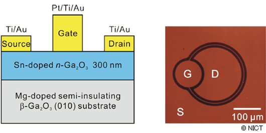
Figure 3: (a) Cross-sectional schematic and (b) optical microscope micrograph of Ga2O3 MESFET.
The output characteristics in Figure 4(a) show an ideal transistor action, represented by the drain current modulation due to the gate voltage (VGS) swing. A complete drain current pinch-off characteristic was also obtained for VGS < −20 V, and the three-terminal off-state breakdown voltage was over 250 V (very high, says the researchers, considering that the device has a simple FET structure without any measures to increase the breakdown voltage). A low drain leakage current of 3μA (several μA/mm) in the off-state led to a high on/off drain current ratio of about 10,000.
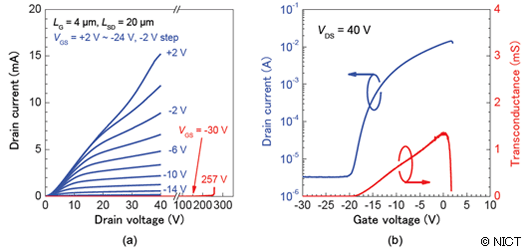
Figure 4: (a) Output and (b) transfer characteristics of Ga2O3 MESFET.
Such device characteristics - obtained at the early stage of development - indicate the great potential of Ga2O3-based electrical devices for future power-device applications, say the researchers, leading to a large reduction in power loss during switching operation and making them suitable for practical power devices.
The work was partially supported by ‘The research and development project for innovation technique of energy conservation’ of Japan’s New Energy and Industrial Technology Development Organization (NEDO).