- News
4 January 2012
InGaAs buffer/channel structure boosts effective mobility 4.2x that of silicon
Researchers in Japan have been using metal-oxide-semiconductor (MOS) interface buffer layers of wider-bandgap material to boost the effective mobility of indium gallium arsenide (InGaAs) channels for future silicon electronics [SangHyeon Kim et al, Appl. Phys. Express, vol5, p014201, 2012].
 The effective electron mobility for 5nm-thick channels was 2810cm2/V-s with a sheet charge carrier density of 1012/cm2. The mobility is enhanced over that for silicon (4.2x), and even over that for InGaAs without top and bottom buffer barriers (1.6x).
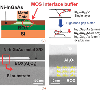
Figure 1: (a) Schematic of In0.7Ga0.3As-OI MOSFETs with a MOS interface buffer layer. Band energy diagram with an electron distribution is also shown. (b) A cross-sectional TEM image of fabricated MOSFET with a Tbody of 2/5/3nm.
“This significant enhancement is attributable to the insertion of the buffer layers and resulting reduction in surface roughness scattering due to the smoother epitaxial-channel interfaces,” the researchers say.
The buffer/barrier interface layers consist of lower indium content InGaAs. Lower indium content tends to widen the bandgap. Other groups have used indium aluminum arsenide (InAlAs) or indium phosphide (InP) to create MOS interface buffer layers designed to reduce the scattering effects that degrade mobility.
The researchers explain their choice of InGaAs: “Here, we have used very thin In0.3Ga0.7As layers as the MOS interface buffer, because of the good MOS interface properties of Al2O3/InGaAs, the relatively large permittivity (~14), and the stable successive-growth condition without epitaxial surface degradation in the growth of InAlAs and InP due to the change of gas species during the epitaxial growth.”
High-mobility channels are seen to be necessary for future (~2015, <16nm) mainstream electronics to achieve the targets of higher performance and lower power consumption.
The research builds on the recent work of the group consisting of The University of Tokyo, the National Institute of Advanced Industrial Science and Technology (NAIST) and Sumitomo Chemical Co Ltd in the direct wafer bonding of III-V-on-insulator (III-V-OI) structures (Increasing performance with III-V transistors on silicon) where effective mobilities of 1700cm2/V-s were achieved.
The researchers grow their epitaxial layers on indium phosphide substrates using metal-organic chemical vapor deposition (MOCVD). The structures are then flipped onto silicon and the InP substrate and some etching sacrificial layers removed.
In the new devices the extremely thin body channel consisted of an In0.7Ga0.3As well sandwiched between In0.3Ga0.7As barriers. The thickness of the body layer was varied (1nm, 3nm, and 5nm) with the top and bottom barriers 2nm and 3nm thick, respectively.
 The source–drain electrodes consisted of Tokyo/NAIST/Sumitomo’s recently developed nickel-InGaAs structures (Self-aligned Ni-InGaAs as source–drain for InGaAs MOSFET). The gate stack was tantalum on high-dielectric-constant insulating aluminum oxide.
The on–off current ratio of 5nm ETB channel devices was found to be ~105 at 1V drain bias. The subthreshold slope was 172mV/dec. The thinnest ETB devices of 1nm were normally operational, despite the hazard of the breaks in the channel, and had improved on–off ratios of 107 and lower subthreshold slopes of 103mV/dec.
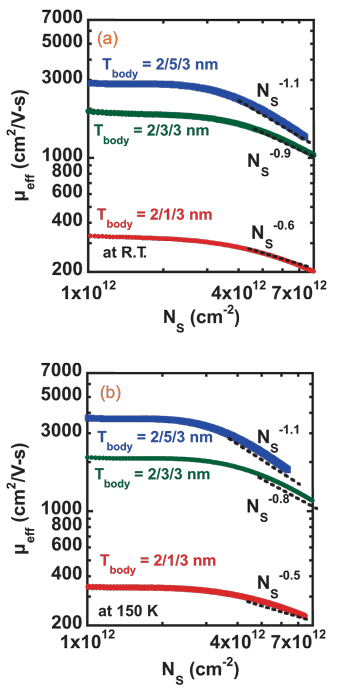
Figure 2: Mobility characteristics of In0.7Ga0.3As-OI MOSFETs with a MOS interface buffer layer with different Tbody values at (a) room temperature and (b) 150K.
The dependence of effective mobility on sheet carrier concentrations was measured at room temperature and at low temperature (150K) to separate phonon scattering from other effects (e.g. interface scattering) in degrading performance (Figure 2).
Although reducing the temperature slightly increased the mobility value, the shapes of the mobility–concentration curves were almost the same. The shapes are attributed to the impacts of a combination of surface roughness and channel-thickness fluctuation. In particular, in thinner channels, fluctuations have more relative impact, severely reducing mobility between 3nm and 1nm.
The researchers conclude: “As a result, in order to reduce the influence of both scattering mechanisms and to achieve higher mobility with Tbody thinner than 10nm, it is very important to form uniform and flat InGaAs-OI layers.”
Increasing performance with III-V transistors on silicon
Self-aligned Ni-InGaAs as source–drain for InGaAs MOSFET
InGaAs buffer/channel structure
The author Mike Cooke is a freelance technology journalist who has worked in the semiconductor and advanced technology sectors since 1997.