- News
23 February 2012
Flattening transconductance profiles in nitride HEMTs
Ohio State University (OSU) researchers have achieved nitride transistors with a flat transconductance profile over a range of gate potentials by using polarization effects [Pil Sung Park et al, Appl. Phys. Lett., vol100, p063507, 2012]. Such transconductance profiles are needed for amplifiers to achieve high linearity and gain simultaneously.
Nitride high-electron-mobility transistors (HEMTs) can achieve high power density and efficiency. Usually in such devices, the transconductance peaks over a very small range of gate potentials, giving a low bandwidth for amplification. These devices use the polarization contrast between gallium nitride and alloys such as aluminum gallium nitride (AlGaN) or indium aluminum nitride (InAlN) to create an extremely thin conducting layer or ‘two dimensional electron gas’ (2DEG) near the interface.
The OSU device uses an AlGaN layer with a composition that is linearly graded between GaN and Al0.15Ga0.85N, followed by a high-Al-content barrier. This expands the thickness of the conducting layer to 5-6nm, giving a quasi-three-dimensional electron gas profile.
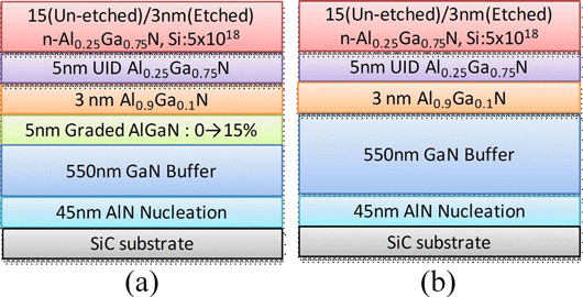
Figure 1: Epitaxial structure of the (a) graded-channel HEMT and (b) conventional HEMT.
The researchers produced two epitaxial structures (Figure 1), grown using plasma-assisted molecular beam epitaxy (PAMBE) on silicon-face 4H-silicon carbide substrates. The silicon-doping of the top layer was designed to improve access in the source-drain regions with low-resistance ohmic contact with a typical titanium/aluminum/nickel/gold alloy stack. The difference between the structures is the inclusion of a 5nm linearly graded composition AlGaN layer for the new device, as opposed to the abrupt junction of the conventional HEMT.
Isolation mesas and gate recessing were created using inductively coupled plasma etch. The gate consisted of a nickel/gold/nickel Schottky contact. The device width was 150μm (2x75μm). The gate length was 1.5μm. The source-gate and drain-gate distances were 1μm and 1.5μm, respectively.
Hall and transmission line model (TLM) measurements suggest a relatively low mobility compared with the more than 1000cm2/V-s of conventional HEMT structures. This was not expected to impact the transconductance profile in the saturation region. Using an AlN cap, rather than Al0.9Ga0.1N, could improve the mobility in both structures, the researchers believe.
The pinch-off voltage of the graded-channel HEMT (-3.2V) was somewhat more negative than for the conventional device (-2.6V), due to the thicker, deeper channel in the former case. The maximum drain currents were 970mA/mm and 720mA/mm for the graded and conventional devices, respectively.
The transconductance for the graded device averaged to 159mS/mm over gate potentials ranging from -2.2V to +3.5V (Figure 2a). The important feature is that, rather than just peaking in transconductance, the graded device profile is approximately flat. The conventional device shows a normal peaking behavior at 159mS/mm. The peak for the graded device was somewhat higher, at 168mS/mm.
The researchers also took account of the relatively high source access resistances of 3Ω and 4.8Ω for the graded and conventional devices, respectively, to estimate the intrinsic transconductance (Figure 2b). These increased the peak values to 318mS/mm for the graded device and 674mS/mm for the conventional HEMT.
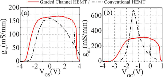
Figure 2: Extrinsic (a) and intrinsic (b) transconductances (gm/gmi) vs gate potential (Vgs/Vgc) for graded-channel and conventional HEMTs at drain bias of 10V.
The researchers comment: “The flat transconductance profile will improve the overall linearity and gain curves of large-signal microwave amplifiers based on these graded-channel devices. In addition to the obvious impact this graded channel design has on linearity, there may be other significant advantages from the nanoscale control of electron density in the channel.”
For example, reducing the electron density can increase velocities. The graded structure could be used to tune electron density while maintaining channel thicknesses that are suitable for high-frequency performance.
The US Office of Naval Research (ONR) and Air Force Research Laboratory (AFRL) provided financial support for the work.
AlGaN/GaN HEMTs PAMBE SiC substrates HEMTs
The author Mike Cooke is a freelance technology journalist who has worked in the semiconductor and advanced technology sectors since 1997.