- News
7 February 2012
Tri-gate applied to make normally-off nitride semiconductor transistors
Massachusetts Institute of Technology (MIT) has applied tri-gate technology to create new normally-off nitride semiconductor transistors, increasing on/off current ratios to eight orders of magnitude and reducing the sub-threshold slope to 86mV/dec on average [Bin Lu et al, IEEE Electron Device Letters, published online 27 January 2012].
The work was partially funded by the Office of Naval Research (ONR) Young Investigator Program and by the US Department of Energy’s Advanced Research Projects Agency Energy (ARPA-E) Agile Delivery of Electrical Power Technology (ADEPT) project (http://arpa-e.energy.gov).
Tri-gate structures, which wrap around the channel, have been used in next-generation development of silicon CMOS circuitry to increase electrostatic control of channel currents and to reduce short-channel effects such as increases in sub-threshold slope and drain-induced barrier lowering.
As applied to nitride semiconductor transistors, the MIT tri-gate device enables normally-off behavior. Conventional nitride semiconductor high-electron-mobility transistors (HEMTs) operate with the current ‘on’ at zero gate potential (normally-on or depletion-mode behavior).
For applications such as power electronics, one needs normally-off (enhancement-mode) behavior for widespread adoption in circuits that need fail-safe operation. Also, normally-off transistor circuits generally consume less power.
Other techniques have been used with varying success to increase the threshold voltage into the normally-off region, such as plasma treatment to shift the band structure of the channel region under the gate and recessing of the gate to bring it nearer to the channel. However these methods tend to degrade the on- and off-current performance. High-voltage-breakdown performance is also a key requirement for power electronics that is not adequately met by existing normally-off nitride transistors.
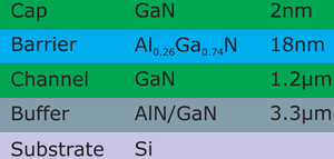 The epitaxial material (Figure 1) was grown on silicon using metal-organic chemical vapor deposition (MOCVD). Device fabrication began with mesa isolation and ohmic contact deposition (Ti/Al/Ni/Au). A trench structure was defined using lithography.
Figure 1: Epitaxial layer structure.
The pattern was defined by a Lloyd’s mirror setup where light is reflected from glass at a small angle, creating a second, virtual source. Combination of the direct and reflected light results in interference fringes, in this case on the photoresist.
The trenches were then etched out using a silicon dioxide mask, giving 660nm depressions at 300nm intervals (Figure 2). The depth of the sidewalls was 250nm and the width of the top channel was 90nm. A normally-off section of channel was then defined by etching 30nm into a 120nm-long section (recessing). The gate dielectric 9nm SiO2 and 7nm of Al2O3 was applied using atomic layer deposition (ALD) after annealing and cleaning/surface treatment steps.
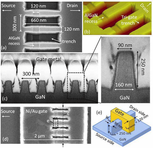
Figure 2: (a) Top-view scanning-electron-microscope (SEM) image of a recessed tri-gate structure before deposition of gate electrode; (b) atomic force microscope (AFM) image of the structure in (a); (c) cross-section SEM image of the tri-gate structure from the cutline in (d); (d) top-view SEM image of the tri-gate normally-off GaN MISFET after the deposition of a 2μm-long gate electrode; (e) Schematic of the normally-off channel region in the square-dashed-line area in (d).
The nickel/gold metal gate was 2μm long. Further annealing at 500°C in nitrogen was carried out to improve the gate dielectric quality. Reference devices with planar structures with the same dielectric and some with gate recessing were also produced.
Averaged over 16 tri-gate devices, the threshold voltage was +0.80V. The drain leakage at 5V bias was 0.3mA/mm at +0.8V gate potential and 1μA/mm at +0.54V. The sub-threshold slope was 86mV/dec at 1V drain bias. The sub-threshold behavior suggested a SiO2/GaN interface trap density of 0.6–1.2x10¹²/cm2-eV. The slope for the planar comparison device was 113mV/dec. The on/off ratio for the tri-gate device was more than eight orders of magnitude (~ factor of 100 million).
One effect of using the SiO2/Al2O3 dielectric combination is to reduce gate leakage to 0.1nA/mm at +7V gate bias. The typical gate dielectric breakdown voltage was 8V.
The maximum current density decreased with source–drain distance. At a distance of 8.5μm, the maximum current density was 530mA/mm at drain bias 10V and gate potential +7V. The tri-gate device had an on-resistance (Ron) of 13.8Ω-mm, compared with the slightly lower value of 12.1Ω-mm of the planar device. The researchers comment: “Further improvement of the Ron is expected by scaling the device channel dimensions and reducing the access-resistance.”
The tri-gate also had improved short-channel performance in terms of drain-induced barrier lowering and constant sub-threshold current and slope, compared with longer-gate-length planar devices (Figure 3). A recessed-gate planar MISFET was not completely off at 0V gate potential, giving a drain current of 28μA/mm at 1V drain bias. The tri-gate device reduced the 0V gate potential 1V drain current to less than 0.5nA/mm.
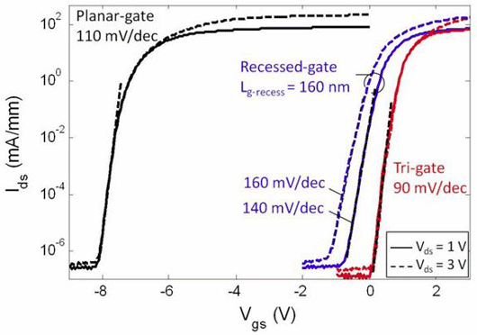
Figure 3: Ids–Vgs characteristics of the tri-gate normally-off MISFET compared with the standard planar-gate transistor and the planar-recessed gate MISFETs with recessed-gate length of 160nm. All the devices have the same dimensions with Lgd = 8μm and are biased at Vds = 1V and 3V.
“The positive shift of the threshold voltage is possibly due to the lateral channel depletion from the sidewalls in the tri-gate structure,” the researchers write.
The 0.6μA/mm breakdown voltage for 0V gate was as high as 565V (gate–drain distance 10μm). The breakdown is described as being ‘hard’ (i.e. permanent), occurring in the gate dielectric.
The researchers comment: “The breakdown voltage of 565V at 0.6μA/mm with Vgs = 0V is an important improvement with respect to other normally-off GaN devices in the literature, typically measured at a much higher drain leakage current level of 0.1-1mA/mm.”
Tri-gate Normally-off nitride transistors MISFET GaN MOCVD
The author Mike Cooke is a freelance technology journalist who has worked in the semiconductor and advanced technology sectors since 1997.