- News
21 February 2012
Avoiding high temperatures and plasma improves InGaAs MOSFET performance
Lund University in Sweden has been developing a low-impact self-aligned process to create metal-oxide semiconductor field-effect transistors (MOSFETs) with high-quality indium gallium arsenide (InGaAs) channels [Mikael Egard et al, IEEE Electron Device Letters, published online 10 February 2012].
InGaAs channels have been proposed as a means towards smaller, better-performing electronic circuits because the material allows faster transport of electrons. However, there are a number of obstacles at present to even meeting the performance of traditional silicon-based devices.
InGaAs MOSFET development is hampered by low quality of the interface with the gate oxide insulator and high access resistance to the source-drain contacts.
The Lund researchers improved the interface quality by using a low-temperature process and wet etching. Compound semiconductors are often etched using faster plasma ‘dry’ etches that can leave rough surfaces and degrade interface quality.
The access resistance was improved through a self-aligned process involving metal-organic chemical vapor deposition (MOCVD) to create source-drain regions without the usual heterostructure barriers to the channel.
The process began by depositing 190nm/5nm/1nm indium aluminum arsenide (InAlAs) buffer/back barrier/spacer and 10nm indium gallium arsenide (InGaAs) channel structures on indium phosphide (100)-oriented substrates using molecular beam epitaxy (MBE) – see Figure 1.
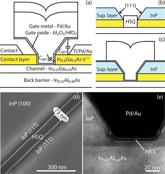
Figure 1: Schematic cross section of (a) the completed device, (b) after MOCVD regrowth, and (c) after deposition of gate metal. (d) Shows a top-view SEM image corresponding to Fig. 1(b), and (e) shows a cross-sectional TEM image corresponding to Fig. 1(c).
Dummy gates of a ‘silicon dioxide-like’ material were formed as a hard mask using electron-beam lithography and hydrogen silsesquioxane (HSQ) resist. The mask was used to allow selective growth of 30nm InGaAs and 90nm InP source-drain layers in an MOCVD deposition process.
The dummy gates were removed in a buffer oxide etch process, leaving the InGaAs channel surface open for the foot of the gate stack to be deposited.
The insulating layers of 0.5nm aluminum oxide (Al2O3) and 6.5nm hafnium dioxide (HfO2) were applied using atomic layer deposition (ALD). The precursors for the aluminum, hafnium and oxygen were trimethyl aluminum (TMA), tetrakis dimethyl amino hafnium (TDMAHf), and water (H2O), respectively.
The gate metal consisted of 10nm palladium (Pd) and 290nm gold (Au). A T-gate structure was added to this by first removing oxide material outside the gate region with a buffered oxide etch, and then selectively etching the InP support layer in hydrochloric acid.
The source/drain contacts were formed using thermal evaporation of titanium, palladium and gold (Ti/Pd/Au). The access resistance of the contacts was estimated to be 156Ω-μm.
At a drain bias of 1V, the current at 1.8V gate potential for a 55nm gate-length device was 2.0mA/mm and the on resistance was a record low of 199Ω-micron. The peak extrinsic transconductance at 0.5V gate potential was 1.9mS/μm. At the lower drain bias of 0.5V, the peak transconductance was 1.5mS/μm and the threshold voltage was -0.3V. Short-channel effects and impact ionization effects resulted in a rather large subthreshold swing value of 187mV/dec.
A 140nm-gate device even showed a marginal ‘enhancement’ behavior with a barely positive threshold voltage of +0.06V at a drain bias of 0.5V. The subthreshold swing was 100mV/dec; the on-off current ratio was 2.4x10³; the peak extrinsic transconductance was 1.05mS/μm; the on-resistance was 265Ω-μm; and the drain-induced barrier lowering was 110mV/V. At the lower drain bias of 0.05V, the subthreshold swing was as low as 79mV/dec. The theoretical minimum for planar devices is 60mV/dec at room temperature.
Capacitance-voltage measurements indicated an interface trap density of 4-8x10¹²/eV-cm2 in the upper part of the energy bandgap. These results, compared with MOS capacitor/diode measurements, indicate that the processing required to produce the gate does not add a significant amount of traps.
Radio-frequency measurements on the 55nm device gave a peak cut-off frequency (ft) of 244GHz and a peak maximum oscillation (fmax) of 293GHz at 1V drain bias. The intrinsic transconductance at 0.5V gate potential was 3.0mS/μm.
The paper also describes a small-signal model that accounts for the frequency response of gate oxide border traps and impact ionization phenomena found in the narrow-bandgap FETs.
InGaAs gate all-arounder demonstrates shortest channel to date
InGaAs buffer/channel structure boosts effective mobility 4.2x that of silicon
Increasing performance with III-V transistors on silicon
Self-aligned Ni-InGaAs as source–drain for InGaAs MOSFET
InGaAs MOSFET InP MOCVD MBE ALD
The author Mike Cooke is a freelance technology journalist who has worked in the semiconductor and advanced technology sectors since 1997.