

- News
28 December 2012
Nanocolumns support monolithic multi-wavelength emission
Sophia University in Tokyo, Japan, has used nanocolumns of nitride semiconductor to produce different emission color LEDs in a single growth process for what is claimed to be the first time [Katsumi Kishino et al, Appl. Phys. Express, vol6, p012101, 2013].
The researchers have been developing a titanium-mask selective-area growth (SAG) technique of indium gallium nitride (InGaN) nanocolumns by rf-plasma-assisted molecular beam epitaxy (rf-MBE). Previous work has demonstrated strong red photoluminescence comparable with green emission.
The diameter of the nanocolumn was found to influence the peak wavelength, with increasing diameter leading to a wavelength shift from blue to red. This shift apparently arises from the beam-shadowing effects where less gallium is incorporated into the crystal structure, creating high-indium-content InGaN wells with narrower bandgap and hence longer-wavelength emission towards the tops of the columns.
In the latest work, the team produced monolithically four regions of nanocolumns with different emission wavelengths (Figure 1). The rf-MBE growth was performed on gallium nitride templates produced on sapphire using metal-organic chemical vapor deposition (MOCVD). The nanocolumns were arranged in triangular arrays with a lattice constant of 400nm. LEDs 1-3 emitted visible light with DC current injection at wavelengths of 544nm (green), 583nm and 597nm (orange), respectively. The wavelengths from previous PL measurements with the same diameter nanocolumns were 520nm, 570nm, 600nm and (for LED 4) 630nm.
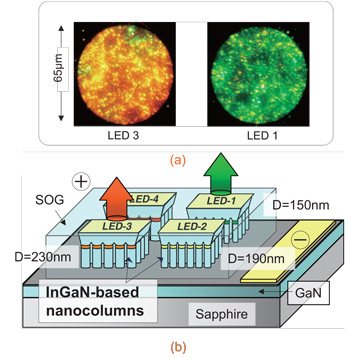 Figure 1: Monolithic integration of InGaN-based nanocolumn LEDs with different emission colors: (a) near-field emission images of green and orange emissions for LEDs 1 and 3, respectively, and (b) schematic diagram of monolithically integrated nanocolumn LEDs on GaN template on sapphire substrate.
The width of the electroluminescence spectrum for LED 2 was broad, at 96nm full-width at half-maximum (FWHM), which was blamed on deficiencies in the SAG process for this region. The other LEDs had narrower emission spectra, with LEDs 1 and 3 having FWHMs of 67nm and 54nm, respectively.
Further imperfections were noted for LED 1 with ‘long-tail’ emission in the yellow region being caused by ‘growth singularities’, and other imperfections such as surface gaps and depressions of the nanocolumn structures that lead to current leakage and other performance degradation. The kink in the green region of the LED 3 is attributed to green emission due to irregular SAG processing, as seen in the near-field image in Figure 1.
Although blue emission is possible in principle, the researchers decided not to produce nanocolumn LEDs for the respective wavelength due to concerns about increased current leakage. The wider spacing between narrower nanocolumns will need sidewall-passivation to suppress such leakage, according to the researchers.
The growth of the nanocolumns proceeded in the order Si-doped n-GaN (3hours at 890°C), InGaN/GaN (1.5nm/1.5nm) short-period superlattice (635-645°C from this point in the process), 3-period InGaN/GaN multi-quantum well (3nm/12nm MQW), 20nm GaN intermediate layer, 10nm p-AlGaN electron blocking, 250nm GaN cladding, and finally a 50nm p-InGaN contact layer.
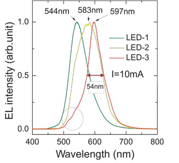 Figure 2: Electroluminescence spectra of LEDs 1–3 under DC current injection of 10mA.
The space between the nanocolumns was filled with spin-on glass (SOG). The p-contact electrodes were formed by etching 70μm-diameter openings in the SOG at the centers of the nanocolumn arrays, depositing indium tin oxide (ITO) transparent conducting material, and titanium/palladium/gold metal electrode layers. Emission windows of 65μm diameter were etched in the p-contact metal. The n-side electrode metals were titanium/aluminium/titanium/gold.
Photoluminescence (PL) of the structures was carried out using a 405nm laser diode excitation. The peak wavelengths were 559nm, 580nm and 590nm for LEDs 1-3, respectively. LED 4 produced little PL. The researchers believe this was due to coalescence of the n-side nanocolumns and the resultant introduction of threading dislocations into the InGaN MQW active region.
LEDs GaN InGaN RF-MBE MOCVD Sapphire substrates
http://apex.jsap.jp/link?APEX/6/012101
The author Mike Cooke is a freelance technology journalist who has worked in the semiconductor and advanced technology sectors since 1997.