

- News
24 December 2012
MIT researchers make smallest working III-V transistors yet
Researchers at Massachusetts Institute of Technology (MIT) have presented the shortest-gate working transistors yet built using III-V channels [J. Lin et al, IEDM, session 32.1]. The metal-oxide-semiconductor field-effect transistors (MOSFETs) were also the first to use self-aligned contacts to reduce the distance between the gate and source-drain regions to 20-30nm. The researchers were keen to reformulate the production processes to more closely resemble those of silicon semiconductor manufacturing. Self-alignment is one such technique.
Matthias Passlack, of Taiwanese semiconductor manufacturer TSMC, commented on the work led by MIT professor Jésus del Alamo: “He and his team have experimentally proven that indium arsenide channels outperform silicon at small-device dimensions. This pioneering work has stimulated and facilitated the development of CMOS-compatible, III-V-based-technology research and development worldwide.”
It is hoped that this research effort will enable use of III-V transistors for future logic and radio-frequency application in high-performance and low-power-consumption electronic devices. The MIT research was funded by US Defense Advanced Research Projects Agency (DARPA), Intel and the Semiconductor Research Corporation’s Center for Materials, Structures and Devices (FCRP-MSD).
The semiconductor material for the MIT device was produced using molecular beam epitaxy (MBE) on indium phosphide (InP) substrates (Figure 1) at Intelliepi. The channel consisted of a quantum well (QW) of indium arsenide (InAs) in indium gallium arsenide (InGaAs) barriers. The upper n+-InP/n+-InAlAs/i-InP layers are a ‘ledge’ designed to lower access resistance between the n+-InGaAs source-drain contact regions and the QW channel.
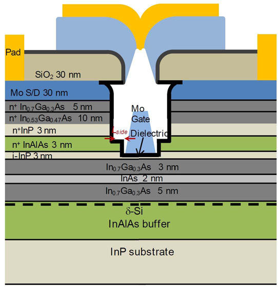
Figure 1: Cross-sectional schematic of InAs QWMOSFET with ultra-scaled HfO2/InP composite barrier.
Sputtered, low-resistance 5Ω/square molybdenum (Mo) was used for metal contacts. This was covered with silicon dioxide (SiO2) in a chemical vapor deposition (CVD) process.
The devices were then patterned with electron-beam lithography and mesa isolation and gate formation achieved with reactive-ion etch (RIE) through the SiO2 and Mo (Figure 2). The RIE damage was repaired using 350°C annealing, the highest temperature used in the entire transistor fabrication process. The gate length was defined by the amount of gate opening, and the researchers believe that this can be scaled to less than 20nm.
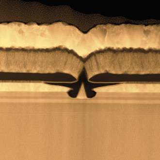 Figure 2: A cross-section transmission electron micrograph of the fabricated transistor. The central inverted V is the gate. The two molybdenum contacts on either side are the source and drain of the transistor. The channel is the InGaAs light color layer under the source, drain and gate. Image courtesy of the MIT researchers.
Further wet and dry etch steps were used to recess the gate region, leaving about 1nm of the 3nm i-InP layer above the top InGaAs barrier of the QW. The control of this last etch was achieved through a self-limiting ‘digital’ technique involving plasma oxidation and dilute sulfuric acid (H2SO4).
The gate dielectric consisted of 2nm hafnium dioxide (HfO2) applied using atomic layer deposition (ALD). The dielectric was deposited conformally and therefore also provided passivation of the access region between the edges of the gate and the n+-InGaAs cap. The dielectric had an equivalent oxide thickness (EOT) of 0.4-0.5nm. The total EOT, including the InP barrier, was ~0.8nm. The Mo gate metal was evaporated on and patterned through etching.
The only lift-off step that was used was pad formation, which would normally be carried out in the backend of line (BEOL) in IC factories.
The researchers found a source-drain resistance of 445Ω-μm, which they describe as “relatively high”, blaming this on the small uncapped regions of the source-drain stacks (Lside in Figure 1). “This can be solved through an improved n+-InP S/D ledge design,” they say.
For a 30nm-gate device, the researchers quote a subthreshold swing of 103mV/dec at 50mV drain and 114mV/dec at 0.5V drain. The drain-induced barrier lowering was “relatively high” at 236mV/V, related to the heterostructure buffer and not the fabrication process.
Despite the HfO2 insulation being very thin at 2nm, gate leakage was less than 1nA/μm.
With 0.5V drain bias, the peak transconductance was 1420μS/μm (1530μS/μm for 60nm-gate). A ‘fully operational’ 22nm-gate device had a peak transconductance of 1050μS/μm with 0.5V drain.
Comparing their device with others (Figure 3), the researchers comment: “Our ultra-scaled barrier MOSFETs exhibit a subthreshold swing that is superior to any other planar III-V MOSFET and that matches the best Tri-gate III-V devices.” Also for sub-60nm-gate transistors, the transconductance performance is “superior to any other planar or Tri-gate III-V MOSFET.”
 Figure 3: Subthreshold swing (S) versus gate length at 0.5V for III-V MOSFETs and high-electron-mobility transistors (HEMTs, essentially transistors without gate insulation).
The researchers also produced a variant device with 15nm InGaAs channel and composite gate dielectric consisting of 0.4nm aluminium oxide and 2nm HfO2. A long-gate (300μm) device achieved a subthreshold swing of 69mV/dec, near to the ideal room-temperature value for planar structures of 60mV/dec. This very low value is among the best ever reported for III-V MOSFETs.
A 20μm-gate device had a mobility of 4650cm2/V-s at a sheet carrier density (Ns) 4x10¹²/cm2. “This is the one of the highest mobility values at this Ns published in InGaAs MOSFETs to date,” the researchers write.
The team plans to next work on improving the electrical performance by reducing the parasitic resistance in these devices. This will enable further shrinking, with the ultimate aim being sub-10nm gate lengths.
InAs QWMOSFET MOSFETs MBE InP substrates Intelliepi InAs InGaAs
www.intelliepi.com/about/index.htm
The author Mike Cooke is a freelance technology journalist who has worked in the semiconductor and advanced technology sectors since 1997.