

- News
13 December 2012
Record-setting 60nm-gate InGaAs MOSFET
Researchers in the USA have achieved record transconductance and cut-off frequencies for indium gallium arsenide (InGaAs) channel metal-oxide field effect transistors (MOSFETs) [D.-H. Kim et al, Appl. Phys. Lett., vol101, p223507, 2012]. The team was based at four organizations: Teledyne Scientific Company, Massachusetts Institute of Technology (MIT), Intelligent Epitaxy Technology, and SEMATECH. The project was financially supported through Teledyne’s internal R&D budget. Funding for MIT came from Intel and the Semiconductor Research Corporation’s Focus Center Research Program.
InGaAs-channel transistors are leading candidates for future complementary oxide semiconductor (CMOS) logic and submillimeter-wave applications.
The molecular-beam epitaxial structure on indium phosphide (InP) substrate consisted of a 300nm back-barrier/buffer of indium aluminium arsenide (In0.52Al0.48As), silicon delta-doping, 5nm In0.52Al0.48As spacer, 10nm indium gallium arsenide (In0.7Ga0.3As) channel, 1nm InP barrier, and a heavily doped multi-layer cap of In0.53Ga0.47As/InP/In0.53Ga0.47As.
The transistor formation included a 2nm gate aluminium oxide (Al2O3) insulator deposited using atomic layer deposition (Figure 1). The device isolation was achieved with a mesa etch. The non-alloyed source-drain contacts were separated by 1μm.
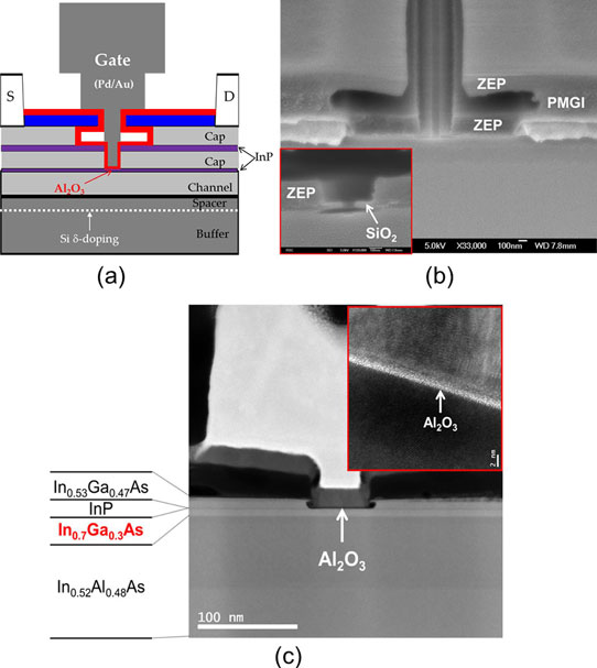
Figure 1: (a) Schematic of recessed In0.7Ga0.3As MOSFET with Al2O3 insulator, (b) SEM image before gate metallization, and (c) TEM image of the fabricated device. Physical gate length (Lg) is 60nm and Al2O3 is 2nm thick, as seen in the inset of (c).
The gate was defined using electron-beam lithographic pattern transfer from ZEP-520A resist into a 20nm silicon dioxide layer. The researchers created a triple-recess palladium/gold gate previously developed by the two lead researchers Dae-Hyun Kim and Jésus A. del Alamo and reported in 2010. At the time, both researchers were with MIT, but Kim has since moved on to Teledyne.
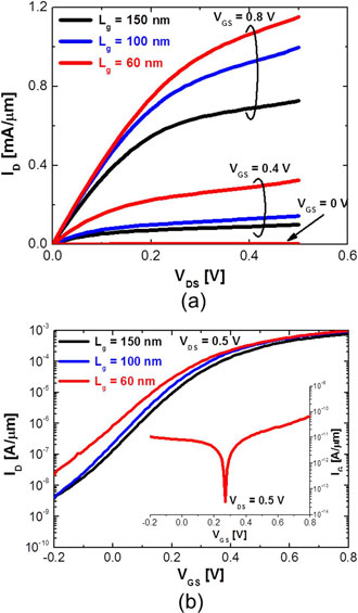 Figure 2: DC characteristics of In0.7Ga0.3As MOSFETs with gate lengths of 150nm, 100nm and 60nm: (a) output characteristics and (b) subthreshold characteristics at 0.5V drain. Inset of (b) is gate current against gate potential for 60nm device.
The gate lengths of the tested transistor varied between 60nm and 150nm. DC measurement (Figure 2) showed that for the 60nm device the on-resistance was fairly low, at 220Ω-μm. The low on-resistance allows the device to achieve the highest maximum transconductance (gm_max) of 2000μS/μm (at 0.5V drain) reported to date for any type of III-V MOSFET.
The threshold voltage of the 60nm transistor was positive, at +0.02V at 0.5V drain bias, giving normally-off enhancement mode behavior. The subthreshold swing is low for InGaAs devices at 110mV/dec, although an even lower value would be desirable. The drain-induced barrier lowering was 200mV/V at 0.5 drain bias.
The researchers compared their transistor with a 75nm gate-length device reported by Intel in 2009 (Table 1). The lower gate leakage current performance for the 60nm device of less than 0.1nA/μm under all bias conditions was delivered by use of improved gate insulation. With an on-current of 0.27mA/μm and off-current of 100nA/μm at 0.5V drain bias, the on/off ratio is more than 1000 (103). For practical devices, this parameter should be higher.
| Lg [nm] |
EOT [nm] |
RON [Ω-μm] |
gm_max [μS/μm] |
fT [GHz] |
S [mV/dec] |
DIBL [mV/V] |
|
| InGaAs MOSFET (this work) | 60 | 1.2 | 220 | 2000 | 370 | 110 | 200 |
| InGaAs MOSFET (Ref. 3) | 75 | 2.2 | 440 | 1750 | N/A | 100 | 130 |
Table 1: Comparison between new 60nm InGaAs MOSFET and 2009 Intel 75nm InGaAs MOSFET at 0.5V drain.
The researchers also measured microwave performance of the 60nm device between 1GHz and 50GHz, finding a current-gain cut-off frequency (fT) of 370GHz and maximum oscillation frequency (fmax) of 280GHz at 0.5V drain and 0.6V gate biases. “This is the highest fT ever reported in any III-V MOSFET on any material system,” the researchers write. The tested device had a gate length of 60nm and a gate width of 2x20μm.
The researchers comment: “The outstanding performance that we demonstrate stems from the triple-recess fabrication process that yields a very tight side recess spacing, coupled with aggressive equivalent oxide thickness (EOT) scaling.”
Further device optimization would focus on creating self-aligned contacts that would reduce device size and deliver a manufacturable process. Such contacts need to be low resistance.
The researchers believe that with such device improvement “the proposed InGaAs MOSFETs with Al2O3 insulator could well become the technology of choice for sub-10nm CMOS logic and THz applications.”
First InGaAs n-MOSFETs on germanium-on-insulator
InGaAs MOSFET InP substrates Intelliepi Teledyne Sematech
http://link.aip.org/link/doi/10.1063/1.4769230
The author Mike Cooke is a freelance technology journalist who has worked in the semiconductor and advanced technology sectors since 1997.