

- News
2 August 2012
Boosting transparent conduction in graphene with gold nanoparticles
Researchers in Korea have been studying how to improve graphene transparent conducting layers (TCLs) using gold nanoparticle (Au-NP) decoration [Minhyeok Choe et al, Appl. Phys. Lett., vol101, p031115, 2012]. The team was variously associated with Gwangju Institute of Science and Technology, Korea Basic Science Institute Jeonju Center, and Seoul National University.
The hopes of those developing graphene for TCL application for light-emitting diodes (LEDs) and solar cells (SCs) is to create current-spreading electrodes with high transparency, conductivity, and flexibility at low cost for volume manufacturing.
Such electrodes are particularly desired for shorter-wavelength nitride semiconductor devices (e.g. for ultraviolet applications), where existing materials such as indium tin oxide (ITO) begin to cut off in transparency. Also, in nitride LEDs current spreading is essential in producing more efficient devices at high output power.
The aim of applying the Au NPs was to control the graphene work-function and conductivity performance. Work-function matching is important in creating high injection currents in LEDs (and hence high output) and low series resistance in SCs (boosting conversion efficiency).
The graphene was formed in a chemical vapor deposition (CVD) process on 300nm-thick polycrystalline nickel on silicon dioxide/silicon (SiO2/Si). The methane source gas was delivered in a hydrogen/argon gas mix. The substrate temperature was 900°C. The multi-layer graphene (MLG) layer was released from the nickel by a wet etch in iron chloride (FeCl3) solution. The Au-NP decoration was achieved through immersion in gold chloride (AuCl3) solution.
The graphene was transferred to nitride semiconductor LEDs and SC epitaxial structures (Figure1) grown using metal-organic chemical vapor deposition (MOCVD) on sapphire. The n-contact regions were exposed by etching with inductively coupled plasma through the p-type gallium nitride (GaN) and indium gallium nitride (InGaN) multi-quantum well (MQW) layers. The MLG was transferred onto the p-GaN. The MLG over the n-contact regions was removed with photolithographic patterning and reactive-ion etch. The n-contact electrode consisted of chromium/gold. The MLG formed a transparent conducting electrode for the p-contact.
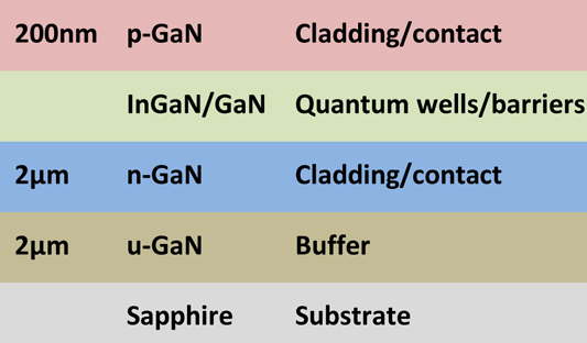
Figure 1: Epitaxial structure of nitride semiconductor LED/SC material. The buffer and n-contact were grown at 1020°C; the multi-quantum wells at 800°C; and, p-contact at 980°C.
Various measurements (UV photoelectron and Raman spectroscopy) on MLGs with Au-NPs suggest a hole-doping effect and an increase in work-function. One negative effect of adding Au-NPs is to reduce transmittance of near-UV 400nm-wavelength light: the transmittance was 89% for MLG without Au-NPs, but 85% for MLG with Au-NPs deposited from a 5mMol/litre (5mM) AuCl3 solution. Increasing the NP density with a 20mM solution further cut transmittance to 78%.
Hall measurements showed a reduction in sheet resistance and an increase in hole density from the application of Au-NPs. The sheet resistance without Au-NPs was ~1000Ω/square, falling to ~200Ω/square and ~100Ω/square for the 5mM and 20mM Au-NP treatments, respectively. The respective hole densities were ~1013/cm3 (no Au-NPs), ~1014/cm3 (5mM), and ~2x10¹⁴/cm3 (20mM).
Further transmission electron microscope (TEM) examination of samples gave the estimated thickness of the MLG as ~9 layers, with an interlayer distance of ~4Å.
The MLG structures were applied as a TCL to nitride semiconductor LEDs (Figure 2). The addition of Au-NPs reduced the forward voltage at 0.4mA to 3.94V (5mM) and 3.86V (20mM) from 4.73V for the TCL without Au-NPs. The reduced forward voltage with Au-NPs is attributed to the smaller work-function difference between TCL and p-GaN allowing high current injection into the MQWs. However, the injection at present is not as good as that obtained with ITO TCLs.
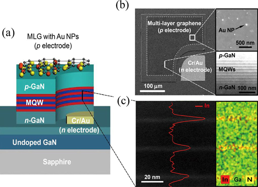
Figure 2: (a) Schematic illustration of MLG-electrode GaN-based LED device. (b) Plan-view SEM image of GaN-based LED device. Insets: SEM image of MLG with Au NPs (top) and TEM image of MQWs (bottom). (c) Magnified TEM image and energy-dispersive x-ray (EDX) mapping of the MQWs.
Electroluminescence (EL) spectra (Figure 3) indicate that the peak wavelength did not shift noticeably with higher current. The best light output performance at 500μA was obtained from 5mM Au-NPs with 94% better performance than without NPs and 29% better performance than the TCL with 20mM Au-NP treatment. The worse light emission performance from the 20mM device is attributed to the reduction in transmittance.
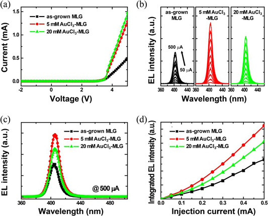
Figure 3: (a) Current-voltage (I-V) curves of GaN-based LEDs with as-grown MLG, 5mM AuCl3-MLG, and 20mM AuCl3-MLG. (b) EL intensity of the MLG-electrode GaN-based LEDs as function of injection current. (c) EL intensity of MLG-electrode GaN-based LEDs measured at 500μA. (d) Integrated EL intensity of MLG-electrode GaN-based LEDs as a function of injection current.
The researchers comment: “By optimizing the concentration of the Au NPs for electrical conductivity and transparency, the current injection and light emission efficiency of the MLG-electrode GaN-based LEDs may be further enhanced.”
For SCs (constructed in same way as the LEDs), the best performance was obtained from 20mM Au-NP MLG. For AM1.5G solar illumination, the short-circuit current was 0.67mA/cm2, the open-circuit voltage was 2.25V, and the fill factor was 0.77, giving a power conversion efficiency of 1.2%. The low level of power conversion is due to the peak response being around 400nm (UV), while the bulk of solar radiation is in the infrared-to-green regions (wavelengths longer than 500nm).
The power conversion for SCs that include MLG electrodes without Au-NPs was around 0.9% (short-circuit current of 0.51mA/cm2). The improved performance for 20mM Au-NPs is attributed to improved conductivity (boosting currents), better light absorption, and lower energy offset between TCL and n-GaN (slightly increasing open-circuit voltage).
Graphene LEDs GaN Sapphire substrates MOCVD
The author Mike Cooke is a freelance technology journalist who has worked in the semiconductor and advanced technology sectors since 1997.