

- News
27 August 2012
Graphene applied to vertical InGaN LEDs to boost output power
Researchers in China have applied graphene as transparent conducting layers (TCLs) in vertical light-emitting diodes (VLEDs) made from indium gallium nitride (InGaN) semiconductors [Liancheng Wang et al, Appl. Phys. Lett., vol101, p061102, 2012]. The researchers were based in Beijing at Chinese Academy of Sciences’ Institute of Semiconductors and Tsinghua University.
Although the use of graphene as a TCL has begun to be explored recently, the application has generally been to more traditional lateral LEDs where the nitride epitaxial material remains attached to its sapphire growth substrate. In a lateral LED, the n- and p-type electrodes are on the same side of the device away from the electrically insulating substrate. The current flow path is therefore partly lateral as it flows through the LED to create light emission.
In the new research, the sapphire substrate was removed using a laser lift-off process to allow vertical current flow from n- and p-type electrodes on opposite sides of the LED chip. In theory, such an arrangement could allow much higher-performance devices, although there is some way to go to make such LEDs more competitive.
One particular problem is the blocking of light output by the metal contacts used to deliver current to the devices. This could be improved by current-spreading layers to re-distribute light output away from the contact region using TCLs such as indium tin oxide (ITO) or graphene. One disadvantage of ITO is poor transparency at shorter wavelengths such as those produced by nitride semiconducting devices (blue-UV). Another problem with ITO is the high cost of indium. Graphene has better transparency characteristics but, apart from being more experimental, its electrical conductivity also tends to be lower.
In the new research, the epitaxial material was grown on sapphire using metal-organic chemical vapor deposition (Figure 1). The u-GaN buffer was 2μm, the n-GaN contact was 5μm, and the p-GaN contact was 0.1μm. The multi-quantum well active region consisted of 10 pairs of 3nm InGaN wells and 7nm GaN barriers.
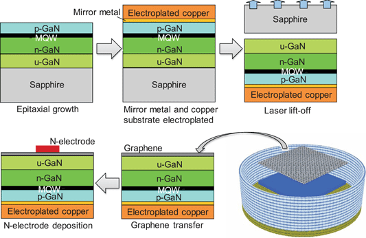
Figure 1. Schematic diagram of G-VLED fabrication process.
After the epitaxial material was grown, a highly reflective metal was deposited on the p-GaN contact layer, followed by electro-deposited copper. The copper eventually became the substrate of the complete VLED. The original sapphire growth substrate was then removed using the laser lift-off process.
The graphene was grown on copper foil in a chemical vapor deposition (CVD) process. The foil was removed using iron chloride solution and the graphene transferred to the flipped GaN layer of the VLED. After drying, the chromium/platinum/gold n-electrode was applied. The VLED chips were isolated and packaged before testing.
The researchers estimate that the resulting graphene consisted of 6 or 7 monolayers. The transmittance of the film was between 85% and 97% in the 400-800nm wavelength range. This compares with ITO with a transmittance in the same range of around 80%.
The result of using graphene (G-VLED) rather than ITO (R-VLED) is a 25% increase in light output (Figure 2). The researchers comment: “The light output improvement of G-VLEDs can be attributed to the higher conductivity of graphene than that of u-GaN. In addition, due to the injection current-spreading characteristics of graphene, G-VLEDs have relatively uniform current distribution, preventing the current accumulating below the N-electrode.”
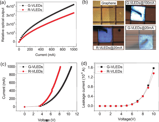
Figure 2. (a) Light output intensity versus current curve for G-VLEDs and R-VLEDs. (b) Emission graph of GVLEDs at different injection currents. (c) Current-voltage characteristics of G-VLEDs and R-VLEDs before annealing. (d) Reverse current-voltage curves of G-VLEDs and R-VLEDs before annealing.
At present, the drawback of graphene is higher forward voltage than the ITO TCL devices (9.35V at 1000mA, compared with 8.21V). The source of the problem is that graphene has a higher contact resistance with u-GaN than ITO.
The forward voltage became higher with annealing. From their measurements, the researchers conclude: “Inter-diffusion of metal atoms and Ga atoms during annealing lead to the partially sandwiched graphene structure, which has been demonstrated to be helpful to improve the performance and reliability of G-VLEDs. It is suggested that more attention needs to be paid to the inter-diffusion of metal atoms between metal pads and GaN, especially when graphene films are extensively used in LEDs as transparent electrodes.”
Some improvement in light output was found with annealing due to higher resistance under the n-electrode spreading and increasing the current density away from the n-electrode that blocks light output.
The author Mike Cooke is a freelance technology journalist who has worked in the semiconductor and advanced technology sectors since 1997.