- News
16 April 2012
Mechanical release of nitride semis from sapphire using boron nitride layer
NTT Basic Research Laboratories in Japan has developed a new method to release nitride semiconductor layers from sapphire substrates [Yasuyuki Kobayashi et al, Nature, vol484, p223, 2012]. Normally slower methods such as laser-lift off or wet etching are used to achieve this.
The new technique uses a thin layer of hexagonal boron nitride (h-BN) between the nitride semiconductors and the sapphire growth substrate. The h-BN has planes of boron and nitrogen bonded in an analog to the sp2-hybridized configuration of carbon (i.e. graphite with strong in-plane bonds but weak plane–plane bonds). This allows for a relatively simple mechanical release of the nitride semiconductor material from the substrate in mere seconds.
 The hexagonal BN (h-BN) is deposited first using metal-organic vapor-phase epitaxy (MOVPE or MOCVD) on sapphire. Triethyl-boron and ammonia (NH3) were used as precursors for the respective elements of h-BN.
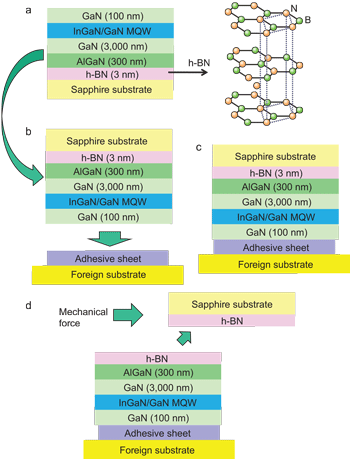
Figure 1: a, Single-crystal h-BN release layer growth is performed on a sapphire substrate, followed by growth of wurtzite AlGaN layer and MQW structure. On right, crystal structure of h-BN is shown. Dotted lines mark unit cell dimensions of h-BN. b, MQW structure is flipped upside down and placed on foreign substrate via adhesive indium sheet. c, MQW structure attached to sheet is heated to a temperature sufficient to heat-seal the indium, and the structure is released from host sapphire by mechanical force and transferred to the foreign substrate (d).
Further layers deposited on the release layer (Figure 1) included a 10-period multi-quantum well structure of InGaN in GaN barriers. The wells were found to be 5.5nm thick with an indium molar content of 15%. The structure was then flipped onto an adhesive indium sheet on a foreign substrate. The combination was then heated to seal the adhesive bond. Finally, the sapphire substrate was separated from the nitride layers using mechanical force. The separation occurs in the h-BN layer and is due to the relative weakness of the plane-plane Van der Waals bonds.
The researchers comment: “In this way, MQWs and other types of nitride devices can be transferred to all kinds of substrates, such as silicon, polycrystalline metal, glass and transparent plastics.”
 It has been found that AlGaN or AlN deposited on the h-BN is needed before the GaN layers to improve the crystal structure and surface properties. Direct growth of GaN on h-BN tends to result in rough, irregular island shapes and polycrystalline structures. One effect of AlGaN/AlN layers on h-BN is as a dislocation filter, reducing the number of threading dislocations in later layers.
The release process takes mere seconds, unlike alternatives such as laser lift-off. The researchers add: “No cracks were observed in the transparent AlGaN/GaN structure up to maximum size of about 1cm square, suggesting that the mechanical release process using the h-BN layer ensures minimal crack formation.”
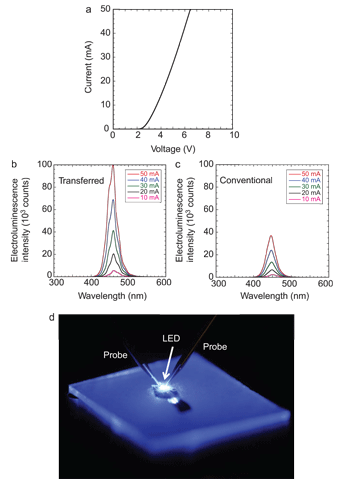
Blue LEDs were produced from the structure with comparable or better performance than LEDs grown on sapphire with AlN buffer (Figure 2).
Figure 2: a, Current–voltage characteristics of transferred LED. b, Electroluminescence spectra from transferred LED. c, Electroluminescence spectra from conventional LED. d, Optical image of blue electroluminescence from transferred vertical-type LED.
Since the new process does not require specialized lift-off equipment or chemical etchants, the researchers see it as leading to considerable cost reduction. Also there is no post-process cleaning, as is needed for laser lift-off. The new mechanical release process leaves a flat surface with root-mean-square roughness of 1nm, considerably lower than laser techniques.
Nitride layers Sapphire substrates Boron nitride LEDs
The author Mike Cooke is a freelance technology journalist who has worked in the semiconductor and advanced technology sectors since 1997.