- News
5 April 2012
InGaAsSbN solar cells grown by MOCVD
Researchers in the USA and Korea have grown heterojunction solar cells with lattice-matched indium gallium arsenide antimonide nitride (InGaAsSbN) base layers using metal-organic chemical vapor deposition (MOCVD) [T. W. Kim et al, Appl. Phys. Lett., vol100, p121120, 2012].
The aim of the work was to create layers with bandgaps around 1eV for incorporation into multi-junction solar cells grown on GaAs substrates. Multi-junction cells have a series of layers with different bandgaps responsive to different regions of the solar spectrum to increase efficiency.
The collaboration consisted of University of Wisconsin-Madison, The Aerospace Corporation, and MicroLink Devices Inc in the USA, and Ajou University in Korea.
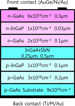 Single-junction solar cells (Figure 1) were grown using metal-organic vapor phase epitaxy (MOVPE, also known as MOCVD). The antimony source was trimethyl-antimony (TMSb) rather than the more usual triethyl-antimony (TESb). Previous experimental work suggests that the use of TESb reduces the nitrogen incorporation in the InGaAsSbN structure. The resulting base regions were found to have compositions given by the formula In0.065Ga0.935As0.9855Sb0.0045N0.01.
The collaboration’s InGaAsSbN material was found to have a carbon background concentration
(9x10¹⁸/cm3) that was significantly higher than for InGaAsN grown under the same conditions. MOCVD growth of InGaAsN(Sb) tends to have 2-3 orders of magnitude greater background carbon. The carbon background could be reduced by using triethyl-gallium as opposed to the trimethyl-gallium used in the collaboration’s structure.
Figure 1: Schematic of InGaAsSbN heterojunction solar cell structure. Two different types of solar cells depend on thickness (sample A, 250nm; sample B, 500nm) of InGaAsSbN base layer.
The base region was also found to have a high hole concentration of 6.5x10¹⁸/cm3, preventing the use of a p-type/intrinsic/n-type (pin) diode structure. Instead, the researchers were forced to use a pn heterojunction.
The material was annealed in a two-step process to improve photoluminescence (PL) performance. The resulting PL spectral peak occurred at 1.04eV at room temperature.
Time-resolved PL was also performed to assess carrier lifetimes. The samples exhibited two decay components: a fast one of tens of picoseconds (78ps for A, 28ps for B), and a slow one of hundreds of picoseconds (576ps for A, 471ps for B). The source of the fast component is still under study but could be due to dislocations. The longer lifetime is consistent with domination by the Shockley-Read-Hall mechanism through trap states.
The 471-576ps lifetime range compares well with the 200ps achieved with InGaAsNSb structures grown using molecular beam epitaxy (MBE) and despite the MOVPE/MOCVD structure having higher background carbon content. MOCVD is preferred over MBE for low-cost manufacturing.
The estimated radiative and Auger recombination lifetimes are at the 5ns and 125ns levels, respectively. A long lifetime is desired to enable the photon-created carriers to be separated and to contribute to generating power. The combined lifetime is dominated by the shortest component – in this case the tens-to-hundreds of picoseconds mechanisms revealed in the time-resolved PL measurement.
Solar cells consisted of the epitaxial material with an active region of 0.2cm2 between the n-type ohmic contact that was arranged in a 0.7μm metal grid with 250μm pitch. The p-type ohmic contact was applied to the back of the material. There was no anti-reflection coating to improve light absoption.
The characteristics of the device (Table 1) suggest that the thicker base layer device (sample B) has higher defect densities, as reflected in the lower open-circuit voltage (Voc). On the positive side, sample B also has a higher short-circuit current (Jsc) due to the increased absorption length.
Base layer |
Voc |
Jsc |
FF |
Efficiency |
250nm |
0.69V |
9.0mA/cm2 |
76.3% |
4.58% |
500nm |
0.59V |
10.9mA/cm2 |
67.0% |
4.09% |
Table 1: Characteristics of solar cells based on sample A (base layer 250nm) and sample B (500nm) under 1 sun AM1.5 direct illumination with entire spectrum range between 35 nm and 1200 nm.
The researchers comment: “The MOVPE-grown InGaAsSbN solar cells reported here exhibit higher Voc and FF (fill factor) values, compared with previously reported InGaAsN solar cells, although higher efficiencies (6.2%) and Jsc (26mA/cm2) have been reported for p-i-n homojunction InGaAsN solar cells.”
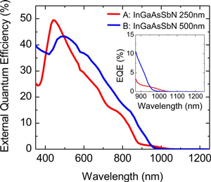 The external quantum efficiency (EQE) was also measured over the spectral range (Figure 2).
Figure 2: Measured spectral external quantum efficiencies of heterojunction InGaAsSbN solar cells with 250nm and 500nm base layers.
The researchers conclude: “Further optimization of the MOVPE growth conditions, including the use of alternate Sb sources, would be required to reduce the background carbon doping concentration in the InGaAsSbN base region and lead to further improvements in device performance”.
The work at UW-Madison was supported under the US Army Research Laboratory (ARL) and US National Science Foundation (NSF) Centers of Excellence for Materials Research and Innovation (CEMRI) finance. The work in Korea was supported by a Korea Institute of Energy Technology Evaluation and Planning Grant.
The Aerospace Corporation is a US Federally funded research & development center (FFRDC) that provides independent technical and scientific research, development, and advisory services to US national-security space programs. MicroLink Devices specializes in MOCVD growth of semiconductor structures for use in wireless communications devices, and the fabrication of advanced solar cells for space, unmanned aerial vehicle (UAV), and terrestrial use.
Solar cells InGaAs solar cells MOCVD MicroLink Devices
The author Mike Cooke is a freelance technology journalist who has worked in the semiconductor and advanced technology sectors since 1997.