- News
26 April 2012
Crack-free nitride semi DBRs
Meijo University and Nagoya University in Japan have grown crack-free nitride semiconductor distributed Bragg reflectors (DBRs) on aluminum nitride (AlN) templates [Kouta Yagi, et al, Jpn. J. Appl. Phys., vol51, p051001, 2012]. This is the first use of AlN templates for nitride DBRs.
Although continuous-wave blue nitride semiconductor vertical-cavity surface-emitting lasers (VCSELs) have finally been produced in the past couple of years, these were based on oxide dielectric DBRs. However, in other material systems advantages have been found in having DBRs constructed from active semiconductor material.
A further attraction of aluminum nitride/gallium nitride (AlN/GaN) semiconductor DBRs would be improved thermal conductivity over typical dielectric structures. However, AlN/GaN DBRs grown on GaN templates tend to crack. The cracks result from the large 2.4% lattice mismatch between AlN and GaN and a large difference in thermal expansion coefficients.
 Expected applications for blue VCSELs include white light sources, printers, and displays.
The Meijo/Nagoya DBRs were grown on AlN and GaN templates on sapphire substrates using low-pressure metal-organic chemical vapor deposition (MOCVD). The 1μm AlN template layer was grown directly on sapphire at 1250°C under a pressure of 26Torr. The comparison 2μm-thick GaN templates were produced using a low-temperature buffer grown at 550°C, followed by high-temperature GaN grown at 1070°C.
The DBR growth on the two types of template was performed simultaneously. The growth conditions were 1040°C temperature and 50Torr pressure. The DBRs were designed with a violet center wavelength of 400nm. The AlN/GaN pairs were optically a quarter-wavelength thick. Structures with 30 and 10 AlN/GaN pairs were produced for comparison. The structures began with quarter wavelength of AlN and ended with quarter wavelength of GaN.
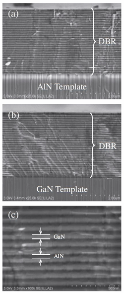
Figure 1: Scanning electron microscope cross-sections of 30-pair AlN/GaN DBRs on (a) AlN and (b) GaN. (c) High-magnification image of DBR on AlN.
A series of analyses of the structure were carried out using electron microscopy (Figure 1) and x-ray diffraction (XRD). The researchers estimated the thickness of the AlN and GaN layers at 40.1nm and 46.0nm, respectively, using XRD measurements. The top 20 AlN/GaN layers of the structure are estimated to be in balanced +1.1% (tensile) and –1.1% (compressive) stress, respectively. The lower 10 layers form the region where the materials relax from the stress imposed by the respective templates.
The use of an AlN template was found to result in DBRs without cracks, unlike with structures grown on GaN templates. This behavior is attributed to the different compressive or tensile stress given by the AlN/GaN templates, respectively. Tension tends to lead to cracking as the main channel for stress relaxation. For compression, other relaxation paths have to be found, such as the generation of misfit dislocations.
The resulting peak reflectivities for the 30-pair DBRs on AlN or GaN templates were 97.5% at 400nm or 94.3% at 397nm, respectively (Figure 2). The stop bandwidths for 50% reflectivity were 28.2nm and 27.6nm for DBR/AlN and DBR/GaN, respectively.
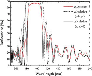 Figure 2: Comparison of measured and calculated reflectivity spectra of 30-pair AlN/GaN DBRs on AlN. Two calculation results are plotted with abrupt AlN/GaN interfaces and with 27nm graded AlGaN layers.
The researchers comment: “Even though these values are still inferior to the expected values, most likely due to the surface and interface roughness, the crack-free AlN/GaN DBRs on AlN will be an important structure for nitride-semiconductor-based blue VCSELs with a high yield.”
The DBR surfaces were rough compared to normal GaN: atomic force microscopy gave 3nm root-mean-square roughness in a 10μm square; the corresponding figure for typical GaN surfaces is less than 1nm. The researchers believe that that their measurements indicate a degree of AlGaN grading between the AlN and GaN layers.
http://jjap.jsap.jp/link?JJAP/51/051001
The author Mike Cooke is a freelance technology journalist who has worked in the semiconductor and advanced technology sectors since 1997.